


1. Overview
The NEORV32 RISC-V Processor is an open-source RISC-V compatible processor system that is intended as ready-to-go auxiliary processor within a larger SoC designs or as stand-alone custom / customizable microcontroller.
The system is highly configurable and provides optional common peripherals like embedded memories, timers, serial interfaces, general purpose IO ports and an external bus interface to connect custom IP like memories, NoCs and other peripherals. On-line and in-system debugging is supported by an OpenOCD/gdb compatible on-chip debugger accessible via JTAG.
Special focus is paid on execution safety to provide defined and predictable behavior at any time. Therefore, the CPU ensures that all memory access are acknowledged and no invalid/malformed instructions are executed. Whenever an unexpected situation occurs, the application code is informed via hardware exceptions.
The software framework of the processor comes with application makefiles, software libraries for all CPU and processor features, a bootloader, a runtime environment and several example programs - including a port of the CoreMark MCU benchmark and the official RISC-V architecture test suite. RISC-V GCC is used as default toolchain.
Check out the processor’s online User Guide that provides hands-on tutorials to get you started.
Structure
1.1. Project Key Features
Project
-
all-in-one package: CPU + SoC + Software Framework & Tooling
-
completely described in behavioral, platform-independent VHDL - no vendor- or technology-specific primitives, attributes, macros, libraries, etc. are used at all
-
all-Verilog "version" available (auto-generated by GHDL)
-
extensive configuration options for adapting the processor to the requirements of the application
-
highly extensible hardware - on CPU, SoC and system level
-
aims to be as small as possible while being as RISC-V-compliant as possible - with a reasonable area-vs-performance trade-off
-
FPGA friendly (e.g. all internal memories can be mapped to block RAM - including the register file)
-
optimized for high clock frequencies to ease timing closure and integration
-
from zero to "hello world!" - completely open source and documented
-
easy to use even for FPGA/RISC-V starters – intended to work out of the box
NEORV32 CPU (the core)
-
32-bit RISC-V CPU
-
fully compatible to the RISC-V ISA specs. - checked by the official RISC-V architecture compatibility tests
-
base ISA + privileged ISA + several optional standard and custom ISA extensions
-
option to add user-defined RISC-V instructions as custom ISA extension
-
rich set of customization options (ISA extensions, design goal: performance / area / energy, tuning options, …)
-
Full Virtualization capabilities to increase execution safety
-
official RISC-V open source architecture ID
NEORV32 Processor (the SoC)
-
highly-configurable full-scale microcontroller-like processor system
-
based on the NEORV32 CPU
-
optional standard serial interfaces (UART, TWI, SPI (host and device), 1-Wire)
-
optional timers and counters (watchdog, system timer)
-
optional general purpose IO and PWM; a native NeoPixel(c)-compatible smart LED interface
-
optional embedded memories and caches for data, instructions and bootloader
-
optional external memory interface for custom connectivity
-
optional DMA controller for CPU-independent data transfers
-
on-chip debugger compatible with OpenOCD and GDB including hardware trigger module and optional authentication
Software framework
-
written in C and based on GCC
-
internal bootloader with serial user interface (via UART)
-
core libraries and HAL for high-level usage of the provided functions and peripherals
-
processor-specific runtime environment and several example programs
-
Doxygen-based documentation of the software framework; a deployed version is available at https://stnolting.github.io/neorv32/sw/files.html
-
Ada support at https://github.com/GNAT-Academic-Program/neorv32-hal
OS Support
-
FreeRTOS port: https://github.com/stnolting/neorv32-freertos
-
Upstream Zephyr support: https://docs.zephyrproject.org/latest/boards/others/neorv32/doc/index.html
-
MicroPython port: https://github.com/stnolting/neorv32-micropython
Extensibility and Customization
The NEORV32 processor is designed to ease customization and extensibility and provides several options for adding application-specific custom hardware modules and accelerators. The three most common options for adding custom on-chip modules are listed below.
-
Processor-External Bus Interface (XBUS) to attach processor-external IP modules (memories and peripherals)
-
Custom Functions Subsystem (CFS) for tightly-coupled processor-internal co-processors
-
Custom Functions Unit (CFU) for custom RISC-V instructions
| A more detailed comparison of the extension/customization options can be found in section Adding Custom Hardware Modules of the user guide. |
1.2. Project Folder Structure
The root directory of the repository is considered the NEORV32 base or home folder (i.e. neorv32/).
neorv32                   - Project home folder
│
├─ docs                   - Documentation
│  ├─ datasheet           - AsciiDoc sources for the NEORV32 data sheet
│  ├─ figures             - Figures and logos
│  └─ userguide           - AsciiDoc sources for the NEORV32 user guide
│
├─ rtl                    - HDL sources
│  ├─ core                - Core sources of the CPU & SoC
│  ├─ system_integration  - System wrappers and bridges for advanced SoC connectivity
│  ├─ test_setups         - Minimal test setup "SoCs" used in the User Guide
│  └─ verilog             - Scripts and examples for converting NEORV32 to Verilog
│
├─ sim                    - Simulation files
│
└─ sw                     - Software framework
   ├─ bootloader          - Sources of the default builtin bootloader
   ├─ common              - Linker script, crt0.S start-up code and central makefile
   ├─ example             - Example programs for the core and the SoC modules
   │  ├─ eclipse          - Pre-configured Eclipse IDE project
   │  └─ ...              - Several example programs
   ├─ image_gen           - Helper program to generate executables & memory images
   ├─ lib                 - NEORV32 core library
   ├─ ocd_firmware        - Firmware for the on-chip debugger "park loop"
   ├─ openocd             - OpenOCD configuration files
   └─ svd                 - Processor system view description file (CMSIS-SVD)
1.3. VHDL File Hierarchy
All required VHDL hardware source files are located in the project’s rtl/core folder.
|
VHDL Library
All core VHDL files from the list below have to be assigned to a new library named neorv32.
|
|
Compilation Order
See section File-List Files for more information.
|
|
Replacing Modules for Customization or Optimization (Especially Memory Modules)
Any module of the core can be replaced for customization purpose.
For ASIC implementations (and for some FPGA implementations), this is particularly recommended for
the underlying memories. Therefore, all (larger) memories are encapsulated as easily replaceable IP
wrappers (i.e. *_ram.vhd and *_rom.vhd files). By default, these wrappers use a generic memory
description that should infer blockRAM on most FPGA platforms.
|
rtl/core
│
├─ neorv32_bootrom.vhd           - Bootloader ROM
├─ neorv32_bootrom_image.vhd     - Bootloader ROM initialization image
├─ neorv32_bootrom_rom.vhd       - Bootloader ROM primitive wrapper
├─ neorv32_bus.vhd               - SoC bus infrastructure modules
├─ neorv32_cache.vhd             - Generic cache module
├─ neorv32_cache_ram.vhd         - Cache tag and data RAM primitive wrapper
├─ neorv32_cfs.vhd               - Custom functions subsystem
├─ neorv32_clint.vhd             - Core local interruptor
├─ neorv32_cpu.vhd               - NEORV32 CPU TOP ENTITY
├─ neorv32_cpu_alu.vhd           - Arithmetic/logic unit
├─ neorv32_cpu_control.vhd       - CPU control, exception system and CSRs
├─ neorv32_cpu_counters.vhd      - Hardware counters (Zicntr & Zihpm ext.)
├─ neorv32_cpu_alu_bitmanip.vhd  - Bit-manipulation unit (B ext.)
├─ neorv32_cpu_alu_cfu.vhd       - Custom instructions unit (Xcfu ext.)
├─ neorv32_cpu_alu_cond.vhd      - Integer conditional unit (Zicond ext.)
├─ neorv32_cpu_alu_crypto.vhd    - Scalar cryptography unit (Zk*/Zbk* ext.)
├─ neorv32_cpu_alu_fpu.vhd       - Floating-point unit (Zfinx ext.)
├─ neorv32_cpu_alu_muldiv.vhd    - Integer MUL/DIV unit (M ext.)
├─ neorv32_cpu_alu_shifter.vhd   - Bit-shift unit (base ISA)
├─ neorv32_cpu_decompressor.vhd  - Compressed instructions decoder (C ext.)
├─ neorv32_cpu_frontend.vhd      - Instruction fetch and issue
├─ neorv32_cpu_hwtrig.vhd        - Hardware trigger module (Sdtrig ext.)
├─ neorv32_cpu_lsu.vhd           - Load/store unit
├─ neorv32_cpu_pmp.vhd           - Physical memory protection unit (Smpmp ext.)
├─ neorv32_cpu_regfile.vhd       - Data register file
├─ neorv32_cpu_trace.vhd         - Trace generator
├─ neorv32_debug_auth.vhd        - On-chip debugger: authentication module
├─ neorv32_debug_dm.vhd          - On-chip debugger: debug module
├─ neorv32_debug_dtm.vhd         - On-chip debugger: debug transfer module
├─ neorv32_dma.vhd               - Direct memory access controller
├─ neorv32_dmem.vhd              - Data memory
├─ neorv32_dmem_ram.vhd          - Data memory RAM primitive wrapper
├─ neorv32_gpio.vhd              - General purpose input/output port unit
├─ neorv32_gptmr.vhd             - General purpose 32-bit timer
├─ neorv32_imem.vhd              - Instruction memory
├─ neorv32_imem_image.vhd        - Instruction memory initialization image
├─ neorv32_imem_ram.vhd          - Instruction memory RAM primitive wrapper
├─ neorv32_imem_rom.vhd          - Instruction memory ROM primitive wrapper
├─ neorv32_neoled.vhd            - NeoPixel (TM) compatible smart LED interface
├─ neorv32_onewire.vhd           - One-Wire serial interface controller
├─ neorv32_package.vhd           - Main VHDL package file
├─ neorv32_prim.vhd              - Generic RTL primitives
├─ neorv32_pwm.vhd               - Pulse-width modulation controller
├─ neorv32_sdi.vhd               - Serial data interface controller (SPI device)
├─ neorv32_slink.vhd             - Stream link interface
├─ neorv32_spi.vhd               - Serial peripheral interface controller (SPI host)
├─ neorv32_sys.vhd               - System infrastructure modules
├─ neorv32_sysinfo.vhd           - System configuration information memory
├─ neorv32_top.vhd               - NEORV32 PROCESSOR/SOC TOP ENTITY
├─ neorv32_tracer.vhd            - Instruction trace buffer
├─ neorv32_trng.vhd              - True random number generator
├─ neorv32_twd.vhd               - Two wire serial device controller
├─ neorv32_twi.vhd               - Two wire serial interface controller
├─ neorv32_uart.vhd              - Universal async. receiver/transmitter
├─ neorv32_wdt.vhd               - Watchdog timer
└─ neorv32_xbus.vhd              - External bus interface gateway
1.3.1. File-List Files
Most of the RTL sources use entity instantiation. Hence, the RTL compile order might be relevant (depending on
the synthesis/simulation tool. Therefore, two file-list files are provided in the rtl folder that list all required
HDL files for the CPU core and for the entire processor and also represent their recommended compile order. Note that
these files list the architecture "bottom-up" - the according top entity is listed in the very last line.
These file-list files can be consumed by EDA tools to simplify project setup.
-
file_list_cpu.f- HDL files and compile order for the CPU core; top module:neorv32_cpu -
file_list_soc.f- HDL files and compile order for the entire processor/SoC; top module:neorv32_top
A simple bash script generate_file_lists.sh is provided for regenerating the file-lists (using GHDL’s elaborate command).
This script can also be invoked using the default application makefile (see Makefile Targets).
By default, the file-list files include a placeholder ($NEORV32_HOME) in the path of each included hardware
source file. These placeholders need to be replaced/substituted by the actual path before being used. Example:
-
default:
$NEORV32_HOME/rtl/core/neorv32_package.vhd -
substituted:
path/to/neorv32/rtl/core/neorv32_package.vhd
Example: Makefile
NEORV32_HOME  ?= path/to/neorv32 (1)
NEORV32_FFILE := $(shell cat $(NEORV32_HOME)/rtl/file_list_soc.f) (2)
NEORV32_SRCS := $(subst $$NEORV32_HOME,$(NEORV32_HOME),$(NEORV32_FFILE)) (3)| 1 | Path to the NEORV32 home folder (i.e. the root folder of the GitHub repository). |
| 2 | Load the content of the file_list_soc.f file-list into a variable NEORV32_SOC_FILE. |
| 3 | Substitute the file-list file’s path placeholder “$NEORV32_HOME” by the actual path and store to NEORV32_SRCS variable. |
Example: TCL
set neorv32_home path/to/neorv32 (1)
set file_list_file [read [open "$neorv32_home/rtl/file_list_soc.f" r]] (2)
set file_list [string map [list {$NEORV32_HOME} $neorv32_home] $file_list_file] (3)| 1 | Path to the NEORV32 home folder (i.e. the root folder of the GitHub repository). |
| 2 | Load the content of the file_list_soc.f file-list into a variable file_list_file. |
| 3 | Substitute the file-list file’s path placeholder “$NEORV32_HOME” by the actual path and store to file_list variable. |
Example: Bash
neorv32/rtl$ export NEORV32_HOME=path/to/neorv32 (1)
neorv32/rtl$ envsubst < file_list_cpu.f > file_list.f (2)| 1 | Set path to the NEORV32 home folder (i.e. the root folder of the GitHub repository) as environment variable. |
| 2 | Substitute $NEORV32_HOME by the content of the according environment variable and store to file_list.f file. |
1.4. VHDL Coding Style
-
The entire processor, including the CPU core, is written in platform-/technology-independent VHDL. The code makes minimal use of VHDL 2008 features in order to remain compatible with older EDA tools.
-
A specific VHDL library
neorv32is used for all sources. -
All registers / flip-flops provide an asynchronous reset (see Processor Reset).
-
The entire setup uses a single clock domain. External "clock" signals are synchronized into this clock domain using 2-stage shift registers.
-
A single package/library file (
neorv32_package.vhd) is used to provide global definitions and auxiliary functions. The user-defined configuration is done entirely via the generics of the top entity. -
Internally, all generics are checked to ensure correct configuration. Asserts are used to inform the user about the actual processor configuration and possible invalid settings.
-
The code uses entity instantiation for all internal modules. However, if multiple submodules are specified within the same source file, component instantiation is used for them. * When instantiating the top-level processor module (
neorv32_top.vhd) in a user-defined design, either entity instantiation or component instantiation can be used, as the NEORV32 package file/library file already provides a corresponding component declaration. -
Larger memories (IMEM, DMEM, caches) are implemented as encapsulated wrappers, which are instantiated by component instantiation. The interfaces of these blocks are static (fixed signal widths; not dependent on the configuration). This means they can be easily replaced by corresponding Verilog IP wrappers (also via black-box instantiation and late binding).
|
All-Verilog Setup
Scripts and instructions for an automatic to-Verilog conversion as well as an all-Verilog
setup that uses custom Verilog memory IPs can be found in rtl/verilog. See
UG: NEORV32 in Verilogfor more information.
|
1.5. Performance
Area Utilization
The NEORV32 processor is optimized for minimal size. However, the actual size (silicon area or FPGA resources)
depends on the specific configuration. For example, an RTOS-capable setup based on a rv32imc_Zicsr_Zicntr CPU
configuration including peripheral and memories requires about 2300 LUTs and 1000 FFs and can run at up to 130 MHz
(implementation results for an Altera Cyclone IV E EP4CE22F17C6 FPGA).
|
NEORV32 Setups
The processor has been successfully ported to AMD, Altera, Lattice, Microchip, Gowin, Cologne Chip
and NanoXplore FPGAs. Some pre-configured example setup are available online: https://github.com/stnolting/neorv32-setups
|
Processing Speed
The computational performance of the NEORV32 is evaluated using Core Mark CPU benchmark. The NEORV32 CoreMark port can be found in a separate repository: neorv32-coremark
| CPU Configuration | CoreMark Score | CoreMarks/MHz |
|---|---|---|
small ( |
33.89 |
0.33 |
medium ( |
62.50 |
0.62 |
performance ( |
95.23 |
0.95 |
dual-core ( |
190.47 |
1.90 |
Performance can be further improved by enabling additional ISA extensions. Note that the compiler
also needs to support these extensions (make sure to use a multilib GCC configuration for optimal
code results).
The NEORV32 CPU is based on a multi-cycle architecture. Each instruction is executed in a sequence of several consecutive micro operations. The average CPI (cycles per instruction) depends on the instruction mix of a specific applications and also on the available CPU extensions, tuning options and memory latency.
1.6. RISC-V Compatibility
The NEORV32 CPU passes the official RISC-V Architectural Certification Tests (ACTs) to "certify it faithfully implements the RISC-V specification". The NEORV32 port of this test framework is available at https://github.com/stnolting/neorv32-riscv-act.
ACT Results for NEORV32 v1.13.2.5, 4th of July, 2026 (click to expand)
RESULT: All 293 tests passed. priv/ExceptionsSm/ExceptionsSm-00.log RVCP-SUMMARY: TEST PASSED - Test File "ExceptionsSm-00.S" priv/ExceptionsU/ExceptionsU-00.log RVCP-SUMMARY: TEST PASSED - Test File "ExceptionsU-00.S" priv/ExceptionsZaamo/ExceptionsZaamo-00.log RVCP-SUMMARY: TEST PASSED - Test File "ExceptionsZaamo-00.S" priv/ExceptionsZalrsc/ExceptionsZalrsc-00.log RVCP-SUMMARY: TEST PASSED - Test File "ExceptionsZalrsc-00.S" priv/ExceptionsZc/ExceptionsZc-00.log RVCP-SUMMARY: TEST PASSED - Test File "ExceptionsZc-00.S" priv/ExceptionsZicboU/ExceptionsZicboU-00.log RVCP-SUMMARY: TEST PASSED - Test File "ExceptionsZicboU-00.S" priv/InterruptsSm/InterruptsSm-00.log RVCP-SUMMARY: TEST PASSED - Test File "InterruptsSm-00.S" priv/InterruptsU/InterruptsU-00.log RVCP-SUMMARY: TEST PASSED - Test File "InterruptsU-00.S" priv/SsstrictSm/SsstrictSm-12.log RVCP-SUMMARY: TEST PASSED - Test File "SsstrictSm-12.S" priv/SsstrictSm/SsstrictSm-13.log RVCP-SUMMARY: TEST PASSED - Test File "SsstrictSm-13.S" priv/SsstrictSm/SsstrictSm-14.log RVCP-SUMMARY: TEST PASSED - Test File "SsstrictSm-14.S" priv/U/U-00.log RVCP-SUMMARY: TEST PASSED - Test File "U-00.S" priv/ZicntrU/ZicntrU-00.log RVCP-SUMMARY: TEST PASSED - Test File "ZicntrU-00.S" priv/pmp/pmp32/PMPSm/pmpsm_all_entries_check.log RVCP-SUMMARY: TEST PASSED - Test File "pmpsm_all_entries_check.S" priv/pmp/pmp32/PMPSm/pmpsm_cfg_A_all.log RVCP-SUMMARY: TEST PASSED - Test File "pmpsm_cfg_A_all.S" priv/pmp/pmp32/PMPSm/pmpsm_cfg_A_off_all.log RVCP-SUMMARY: TEST PASSED - Test File "pmpsm_cfg_A_off_all.S" priv/pmp/pmp32/PMPSm/pmpsm_cfg_A_tor_bot.log RVCP-SUMMARY: TEST PASSED - Test File "pmpsm_cfg_A_tor_bot.S" priv/pmp/pmp32/PMPSm/pmpsm_cfg_A_tor_zero.log RVCP-SUMMARY: TEST PASSED - Test File "pmpsm_cfg_A_tor_zero.S" priv/pmp/pmp32/PMPSm/pmpsm_cfg_L_access_all.log RVCP-SUMMARY: TEST PASSED - Test File "pmpsm_cfg_L_access_all.S" priv/pmp/pmp32/PMPSm/pmpsm_cfg_L_modify_napot.log RVCP-SUMMARY: TEST PASSED - Test File "pmpsm_cfg_L_modify_napot.S" priv/pmp/pmp32/PMPSm/pmpsm_cfg_L_modify_off.log RVCP-SUMMARY: TEST PASSED - Test File "pmpsm_cfg_L_modify_off.S" priv/pmp/pmp32/PMPSm/pmpsm_cfg_L_modify_tor.log RVCP-SUMMARY: TEST PASSED - Test File "pmpsm_cfg_L_modify_tor.S" priv/pmp/pmp32/PMPSm/pmpsm_cfg_XWR_all-01.log RVCP-SUMMARY: TEST PASSED - Test File "pmpsm_cfg_XWR_all-01.S" priv/pmp/pmp32/PMPSm/pmpsm_cfg_XWR_all-02.log RVCP-SUMMARY: TEST PASSED - Test File "pmpsm_cfg_XWR_all-02.S" priv/pmp/pmp32/PMPSm/pmpsm_cfg_XWR_all-03.log RVCP-SUMMARY: TEST PASSED - Test File "pmpsm_cfg_XWR_all-03.S" priv/pmp/pmp32/PMPSm/pmpsm_cfg_XWR_all-04.log RVCP-SUMMARY: TEST PASSED - Test File "pmpsm_cfg_XWR_all-04.S" priv/pmp/pmp32/PMPSm/pmpsm_cfg_napot_all.log RVCP-SUMMARY: TEST PASSED - Test File "pmpsm_cfg_napot_all.S" priv/pmp/pmp32/PMPSm/pmpsm_cfg_tor_all.log RVCP-SUMMARY: TEST PASSED - Test File "pmpsm_cfg_tor_all.S" priv/pmp/pmp32/PMPSm/pmpsm_cfg_tor_check-01.log RVCP-SUMMARY: TEST PASSED - Test File "pmpsm_cfg_tor_check-01.S" priv/pmp/pmp32/PMPSm/pmpsm_cfg_tor_check-02.log RVCP-SUMMARY: TEST PASSED - Test File "pmpsm_cfg_tor_check-02.S" priv/pmp/pmp32/PMPSm/pmpsm_cfg_tor_check-03.log RVCP-SUMMARY: TEST PASSED - Test File "pmpsm_cfg_tor_check-03.S" priv/pmp/pmp32/PMPSm/pmpsm_csr_walk-1.log RVCP-SUMMARY: TEST PASSED - Test File "pmpsm_csr_walk-01.S" priv/pmp/pmp32/PMPSm/pmpsm_csr_walk-10.log RVCP-SUMMARY: TEST PASSED - Test File "pmpsm_csr_walk-10.S" priv/pmp/pmp32/PMPSm/pmpsm_csr_walk-2.log RVCP-SUMMARY: TEST PASSED - Test File "pmpsm_csr_walk-02.S" priv/pmp/pmp32/PMPSm/pmpsm_csr_walk-3.log RVCP-SUMMARY: TEST PASSED - Test File "pmpsm_csr_walk-03.S" priv/pmp/pmp32/PMPSm/pmpsm_csr_walk-4.log RVCP-SUMMARY: TEST PASSED - Test File "pmpsm_csr_walk-04.S" priv/pmp/pmp32/PMPSm/pmpsm_csr_walk-5.log RVCP-SUMMARY: TEST PASSED - Test File "pmpsm_csr_walk-05.S" priv/pmp/pmp32/PMPSm/pmpsm_csr_walk-6.log RVCP-SUMMARY: TEST PASSED - Test File "pmpsm_csr_walk-06.S" priv/pmp/pmp32/PMPSm/pmpsm_csr_walk-7.log RVCP-SUMMARY: TEST PASSED - Test File "pmpsm_csr_walk-07.S" priv/pmp/pmp32/PMPSm/pmpsm_csr_walk-8.log RVCP-SUMMARY: TEST PASSED - Test File "pmpsm_csr_walk-08.S" priv/pmp/pmp32/PMPSm/pmpsm_csr_walk-9.log RVCP-SUMMARY: TEST PASSED - Test File "pmpsm_csr_walk-09.S" priv/pmp/pmp32/PMPSm/pmpsm_grain.log RVCP-SUMMARY: TEST PASSED - Test File "pmpsm_grain.S" priv/pmp/pmp32/PMPSm/pmpsm_grain_check.log RVCP-SUMMARY: TEST PASSED - Test File "pmpsm_grain_check.S" priv/pmp/pmp32/PMPSm/pmpsm_napot_legal_lwxr.log RVCP-SUMMARY: TEST PASSED - Test File "pmpsm_napot_legal_lwxr.S" priv/pmp/pmp32/PMPSm/pmpsm_priority.log RVCP-SUMMARY: TEST PASSED - Test File "pmpsm_priority.S" priv/pmp/pmp32/PMPSm/pmpsm_priority_off.log RVCP-SUMMARY: TEST PASSED - Test File "pmpsm_priority_off.S" priv/pmp/pmp32/PMPSm/pmpsm_tor_legal_lwxr.log RVCP-SUMMARY: TEST PASSED - Test File "pmpsm_tor_legal_lwxr.S" priv/pmp/pmp32/PMPU/pmpu_cfg_A_off.log RVCP-SUMMARY: TEST PASSED - Test File "pmpu_cfg_A_all.S" priv/pmp/pmp32/PMPU/pmpu_cfg_XWR.log RVCP-SUMMARY: TEST PASSED - Test File "pmpu_cfg_XWR.S" priv/pmp/pmp32/PMPU/pmpu_csr_access.log RVCP-SUMMARY: TEST PASSED - Test File "pmpu_csr_access.S" priv/pmp/pmp32/PMPU/pmpu_mprv_check-01.log RVCP-SUMMARY: TEST PASSED - Test File "pmpu_mprv_check-01.S" priv/pmp/pmp32/PMPU/pmpu_mprv_check-02.log RVCP-SUMMARY: TEST PASSED - Test File "pmpu_mprv_check-02.S" priv/pmp/pmp32/PMPU/pmpu_napot_legal_lxwr-01.log RVCP-SUMMARY: TEST PASSED - Test File "pmpu_napot_legal_lxwr.S" priv/pmp/pmp32/PMPU/pmpu_napot_legal_lxwr-02.log RVCP-SUMMARY: TEST PASSED - Test File "pmps_napot_legal_lxwr.S" priv/pmp/pmp32/PMPU/pmpu_tor_legal_lxwr.log RVCP-SUMMARY: TEST PASSED - Test File "pmpu_tor_legal_lxwr.S" priv/pmp/pmp32/PMPZaamo/pmpzaamo_cfg_wr.log RVCP-SUMMARY: TEST PASSED - Test File "pmpzaamo_cfg_wr.S" priv/pmp/pmp32/PMPZalrsc/pmpzalrsc_cfg_wr.log RVCP-SUMMARY: TEST PASSED - Test File "pmpzalrsc_cfg_wrS" priv/pmp/pmp32/PMPZca/pmpzca_aligned_napot.log RVCP-SUMMARY: TEST PASSED - Test File "pmpzca_aligned_napot.S" priv/pmp/pmp32/PMPZca/pmpzca_aligned_off.log RVCP-SUMMARY: TEST PASSED - Test File "pmpzca_aligned_tor.S" priv/pmp/pmp32/PMPZca/pmpzca_aligned_tor.log RVCP-SUMMARY: TEST PASSED - Test File "pmpzca_aligned_tor.S" priv/pmp/pmp32/PMPZca/pmpzca_cret_napot.log RVCP-SUMMARY: TEST PASSED - Test File "pmpzca_cret_napot.S" priv/pmp/pmp32/PMPZca/pmpzca_cret_tor.log RVCP-SUMMARY: TEST PASSED - Test File "pmpzca_cret_napot.S" priv/pmp/pmp32/PMPZca/pmpzca_legal_lwrx.log RVCP-SUMMARY: TEST PASSED - Test File "pmpzca_legal_lxwr.S" priv/pmp/pmp32/PMPZca/pmpzca_misaligned_napot.log RVCP-SUMMARY: TEST PASSED - Test File "pmpzca_misaligned_napot.S" priv/pmp/pmp32/PMPZca/pmpzca_misaligned_off.log RVCP-SUMMARY: TEST PASSED - Test File "pmpzca_misaligned_off.S" priv/pmp/pmp32/PMPZca/pmpzca_misaligned_tor.log RVCP-SUMMARY: TEST PASSED - Test File "pmpzca_misaligned_tor.S" priv/pmp/pmp32/PMPZca/pmpzcb_legal_lxwr.log RVCP-SUMMARY: TEST PASSED - Test File "pmpzcb_legal_lwxr.S" rv32i/I/I-add-00.log RVCP-SUMMARY: TEST PASSED - Test File "I-add-00.S" rv32i/I/I-addi-00.log RVCP-SUMMARY: TEST PASSED - Test File "I-addi-00.S" rv32i/I/I-and-00.log RVCP-SUMMARY: TEST PASSED - Test File "I-and-00.S" rv32i/I/I-andi-00.log RVCP-SUMMARY: TEST PASSED - Test File "I-andi-00.S" rv32i/I/I-auipc-00.log RVCP-SUMMARY: TEST PASSED - Test File "I-auipc-00.S" rv32i/I/I-beq-00.log RVCP-SUMMARY: TEST PASSED - Test File "I-beq-00.S" rv32i/I/I-bge-00.log RVCP-SUMMARY: TEST PASSED - Test File "I-bge-00.S" rv32i/I/I-bgeu-00.log RVCP-SUMMARY: TEST PASSED - Test File "I-bgeu-00.S" rv32i/I/I-blt-00.log RVCP-SUMMARY: TEST PASSED - Test File "I-blt-00.S" rv32i/I/I-bltu-00.log RVCP-SUMMARY: TEST PASSED - Test File "I-bltu-00.S" rv32i/I/I-bne-00.log RVCP-SUMMARY: TEST PASSED - Test File "I-bne-00.S" rv32i/I/I-fence-00.log RVCP-SUMMARY: TEST PASSED - Test File "I-fence-00.S" rv32i/I/I-jal-00.log RVCP-SUMMARY: TEST PASSED - Test File "I-jal-00.S" rv32i/I/I-jalr-00.log RVCP-SUMMARY: TEST PASSED - Test File "I-jalr-00.S" rv32i/I/I-lb-00.log RVCP-SUMMARY: TEST PASSED - Test File "I-lb-00.S" rv32i/I/I-lbu-00.log RVCP-SUMMARY: TEST PASSED - Test File "I-lbu-00.S" rv32i/I/I-lh-00.log RVCP-SUMMARY: TEST PASSED - Test File "I-lh-00.S" rv32i/I/I-lhu-00.log RVCP-SUMMARY: TEST PASSED - Test File "I-lhu-00.S" rv32i/I/I-lui-00.log RVCP-SUMMARY: TEST PASSED - Test File "I-lui-00.S" rv32i/I/I-lw-00.log RVCP-SUMMARY: TEST PASSED - Test File "I-lw-00.S" rv32i/I/I-nop-00.log RVCP-SUMMARY: TEST PASSED - Test File "I-nop-00.S" rv32i/I/I-or-00.log RVCP-SUMMARY: TEST PASSED - Test File "I-or-00.S" rv32i/I/I-ori-00.log RVCP-SUMMARY: TEST PASSED - Test File "I-ori-00.S" rv32i/I/I-sb-00.log RVCP-SUMMARY: TEST PASSED - Test File "I-sb-00.S" rv32i/I/I-sh-00.log RVCP-SUMMARY: TEST PASSED - Test File "I-sh-00.S" rv32i/I/I-sll-00.log RVCP-SUMMARY: TEST PASSED - Test File "I-sll-00.S" rv32i/I/I-slli-00.log RVCP-SUMMARY: TEST PASSED - Test File "I-slli-00.S" rv32i/I/I-slt-00.log RVCP-SUMMARY: TEST PASSED - Test File "I-slt-00.S" rv32i/I/I-slti-00.log RVCP-SUMMARY: TEST PASSED - Test File "I-slti-00.S" rv32i/I/I-sltiu-00.log RVCP-SUMMARY: TEST PASSED - Test File "I-sltiu-00.S" rv32i/I/I-sltu-00.log RVCP-SUMMARY: TEST PASSED - Test File "I-sltu-00.S" rv32i/I/I-sra-00.log RVCP-SUMMARY: TEST PASSED - Test File "I-sra-00.S" rv32i/I/I-srai-00.log RVCP-SUMMARY: TEST PASSED - Test File "I-srai-00.S" rv32i/I/I-srl-00.log RVCP-SUMMARY: TEST PASSED - Test File "I-srl-00.S" rv32i/I/I-srli-00.log RVCP-SUMMARY: TEST PASSED - Test File "I-srli-00.S" rv32i/I/I-sub-00.log RVCP-SUMMARY: TEST PASSED - Test File "I-sub-00.S" rv32i/I/I-sw-00.log RVCP-SUMMARY: TEST PASSED - Test File "I-sw-00.S" rv32i/I/I-xor-00.log RVCP-SUMMARY: TEST PASSED - Test File "I-xor-00.S" rv32i/I/I-xori-00.log RVCP-SUMMARY: TEST PASSED - Test File "I-xori-00.S" rv32i/M/M-div-00.log RVCP-SUMMARY: TEST PASSED - Test File "M-div-00.S" rv32i/M/M-divu-00.log RVCP-SUMMARY: TEST PASSED - Test File "M-divu-00.S" rv32i/M/M-mul-00.log RVCP-SUMMARY: TEST PASSED - Test File "M-mul-00.S" rv32i/M/M-mulh-00.log RVCP-SUMMARY: TEST PASSED - Test File "M-mulh-00.S" rv32i/M/M-mulhsu-00.log RVCP-SUMMARY: TEST PASSED - Test File "M-mulhsu-00.S" rv32i/M/M-mulhu-00.log RVCP-SUMMARY: TEST PASSED - Test File "M-mulhu-00.S" rv32i/M/M-rem-00.log RVCP-SUMMARY: TEST PASSED - Test File "M-rem-00.S" rv32i/M/M-remu-00.log RVCP-SUMMARY: TEST PASSED - Test File "M-remu-00.S" rv32i/Zaamo/Zaamo-amoadd.w-00.log RVCP-SUMMARY: TEST PASSED - Test File "Zaamo-amoadd.w-00.S" rv32i/Zaamo/Zaamo-amoand.w-00.log RVCP-SUMMARY: TEST PASSED - Test File "Zaamo-amoand.w-00.S" rv32i/Zaamo/Zaamo-amomax.w-00.log RVCP-SUMMARY: TEST PASSED - Test File "Zaamo-amomax.w-00.S" rv32i/Zaamo/Zaamo-amomaxu.w-00.log RVCP-SUMMARY: TEST PASSED - Test File "Zaamo-amomaxu.w-00.S" rv32i/Zaamo/Zaamo-amomin.w-00.log RVCP-SUMMARY: TEST PASSED - Test File "Zaamo-amomin.w-00.S" rv32i/Zaamo/Zaamo-amominu.w-00.log RVCP-SUMMARY: TEST PASSED - Test File "Zaamo-amominu.w-00.S" rv32i/Zaamo/Zaamo-amoor.w-00.log RVCP-SUMMARY: TEST PASSED - Test File "Zaamo-amoor.w-00.S" rv32i/Zaamo/Zaamo-amoswap.w-00.log RVCP-SUMMARY: TEST PASSED - Test File "Zaamo-amoswap.w-00.S" rv32i/Zaamo/Zaamo-amoxor.w-00.log RVCP-SUMMARY: TEST PASSED - Test File "Zaamo-amoxor.w-00.S" rv32i/Zalrsc/Zalrsc-lr.w-00.log RVCP-SUMMARY: TEST PASSED - Test File "Zalrsc-lr.w-00.S" rv32i/Zalrsc/Zalrsc-sc.w-00.log RVCP-SUMMARY: TEST PASSED - Test File "Zalrsc-sc.w-00.S" rv32i/Zba/Zba-sh1add-00.log RVCP-SUMMARY: TEST PASSED - Test File "Zba-sh1add-00.S" rv32i/Zba/Zba-sh2add-00.log RVCP-SUMMARY: TEST PASSED - Test File "Zba-sh2add-00.S" rv32i/Zba/Zba-sh3add-00.log RVCP-SUMMARY: TEST PASSED - Test File "Zba-sh3add-00.S" rv32i/Zbb/Zbb-andn-00.log RVCP-SUMMARY: TEST PASSED - Test File "Zbb-andn-00.S" rv32i/Zbb/Zbb-clz-00.log RVCP-SUMMARY: TEST PASSED - Test File "Zbb-clz-00.S" rv32i/Zbb/Zbb-cpop-00.log RVCP-SUMMARY: TEST PASSED - Test File "Zbb-cpop-00.S" rv32i/Zbb/Zbb-ctz-00.log RVCP-SUMMARY: TEST PASSED - Test File "Zbb-ctz-00.S" rv32i/Zbb/Zbb-max-00.log RVCP-SUMMARY: TEST PASSED - Test File "Zbb-max-00.S" rv32i/Zbb/Zbb-maxu-00.log RVCP-SUMMARY: TEST PASSED - Test File "Zbb-maxu-00.S" rv32i/Zbb/Zbb-min-00.log RVCP-SUMMARY: TEST PASSED - Test File "Zbb-min-00.S" rv32i/Zbb/Zbb-minu-00.log RVCP-SUMMARY: TEST PASSED - Test File "Zbb-minu-00.S" rv32i/Zbb/Zbb-orc.b-00.log RVCP-SUMMARY: TEST PASSED - Test File "Zbb-orc.b-00.S" rv32i/Zbb/Zbb-orn-00.log RVCP-SUMMARY: TEST PASSED - Test File "Zbb-orn-00.S" rv32i/Zbb/Zbb-rev8-00.log RVCP-SUMMARY: TEST PASSED - Test File "Zbb-rev8-00.S" rv32i/Zbb/Zbb-rol-00.log RVCP-SUMMARY: TEST PASSED - Test File "Zbb-rol-00.S" rv32i/Zbb/Zbb-ror-00.log RVCP-SUMMARY: TEST PASSED - Test File "Zbb-ror-00.S" rv32i/Zbb/Zbb-rori-00.log RVCP-SUMMARY: TEST PASSED - Test File "Zbb-rori-00.S" rv32i/Zbb/Zbb-sext.b-00.log RVCP-SUMMARY: TEST PASSED - Test File "Zbb-sext.b-00.S" rv32i/Zbb/Zbb-sext.h-00.log RVCP-SUMMARY: TEST PASSED - Test File "Zbb-sext.h-00.S" rv32i/Zbb/Zbb-xnor-00.log RVCP-SUMMARY: TEST PASSED - Test File "Zbb-xnor-00.S" rv32i/Zbb/Zbb-zext.h-00.log RVCP-SUMMARY: TEST PASSED - Test File "Zbb-zext.h-00.S" rv32i/Zbc/Zbc-clmul-00.log RVCP-SUMMARY: TEST PASSED - Test File "Zbc-clmul-00.S" rv32i/Zbc/Zbc-clmulh-00.log RVCP-SUMMARY: TEST PASSED - Test File "Zbc-clmulh-00.S" rv32i/Zbc/Zbc-clmulr-00.log RVCP-SUMMARY: TEST PASSED - Test File "Zbc-clmulr-00.S" rv32i/Zbkb/Zbkb-andn-00.log RVCP-SUMMARY: TEST PASSED - Test File "Zbkb-andn-00.S" rv32i/Zbkb/Zbkb-brev8-00.log RVCP-SUMMARY: TEST PASSED - Test File "Zbkb-brev8-00.S" rv32i/Zbkb/Zbkb-orn-00.log RVCP-SUMMARY: TEST PASSED - Test File "Zbkb-orn-00.S" rv32i/Zbkb/Zbkb-pack-00.log RVCP-SUMMARY: TEST PASSED - Test File "Zbkb-pack-00.S" rv32i/Zbkb/Zbkb-packh-00.log RVCP-SUMMARY: TEST PASSED - Test File "Zbkb-packh-00.S" rv32i/Zbkb/Zbkb-rev8-00.log RVCP-SUMMARY: TEST PASSED - Test File "Zbkb-rev8-00.S" rv32i/Zbkb/Zbkb-rol-00.log RVCP-SUMMARY: TEST PASSED - Test File "Zbkb-rol-00.S" rv32i/Zbkb/Zbkb-ror-00.log RVCP-SUMMARY: TEST PASSED - Test File "Zbkb-ror-00.S" rv32i/Zbkb/Zbkb-rori-00.log RVCP-SUMMARY: TEST PASSED - Test File "Zbkb-rori-00.S" rv32i/Zbkb/Zbkb-unzip-00.log RVCP-SUMMARY: TEST PASSED - Test File "Zbkb-unzip-00.S" rv32i/Zbkb/Zbkb-xnor-00.log RVCP-SUMMARY: TEST PASSED - Test File "Zbkb-xnor-00.S" rv32i/Zbkb/Zbkb-zip-00.log RVCP-SUMMARY: TEST PASSED - Test File "Zbkb-zip-00.S" rv32i/Zbkc/Zbkc-clmul-00.log RVCP-SUMMARY: TEST PASSED - Test File "Zbkc-clmul-00.S" rv32i/Zbkc/Zbkc-clmulh-00.log RVCP-SUMMARY: TEST PASSED - Test File "Zbkc-clmulh-00.S" rv32i/Zbkx/Zbkx-xperm4-00.log RVCP-SUMMARY: TEST PASSED - Test File "Zbkx-xperm4-00.S" rv32i/Zbkx/Zbkx-xperm8-00.log RVCP-SUMMARY: TEST PASSED - Test File "Zbkx-xperm8-00.S" rv32i/Zbs/Zbs-bclr-00.log RVCP-SUMMARY: TEST PASSED - Test File "Zbs-bclr-00.S" rv32i/Zbs/Zbs-bclri-00.log RVCP-SUMMARY: TEST PASSED - Test File "Zbs-bclri-00.S" rv32i/Zbs/Zbs-bext-00.log RVCP-SUMMARY: TEST PASSED - Test File "Zbs-bext-00.S" rv32i/Zbs/Zbs-bexti-00.log RVCP-SUMMARY: TEST PASSED - Test File "Zbs-bexti-00.S" rv32i/Zbs/Zbs-binv-00.log RVCP-SUMMARY: TEST PASSED - Test File "Zbs-binv-00.S" rv32i/Zbs/Zbs-binvi-00.log RVCP-SUMMARY: TEST PASSED - Test File "Zbs-binvi-00.S" rv32i/Zbs/Zbs-bset-00.log RVCP-SUMMARY: TEST PASSED - Test File "Zbs-bset-00.S" rv32i/Zbs/Zbs-bseti-00.log RVCP-SUMMARY: TEST PASSED - Test File "Zbs-bseti-00.S" rv32i/Zca/Zca-c.add-00.log RVCP-SUMMARY: TEST PASSED - Test File "Zca-c.add-00.S" rv32i/Zca/Zca-c.addi-00.log RVCP-SUMMARY: TEST PASSED - Test File "Zca-c.addi-00.S" rv32i/Zca/Zca-c.addi16sp-00.log RVCP-SUMMARY: TEST PASSED - Test File "Zca-c.addi16sp-00.S" rv32i/Zca/Zca-c.addi4spn-00.log RVCP-SUMMARY: TEST PASSED - Test File "Zca-c.addi4spn-00.S" rv32i/Zca/Zca-c.and-00.log RVCP-SUMMARY: TEST PASSED - Test File "Zca-c.and-00.S" rv32i/Zca/Zca-c.andi-00.log RVCP-SUMMARY: TEST PASSED - Test File "Zca-c.andi-00.S" rv32i/Zca/Zca-c.beqz-00.log RVCP-SUMMARY: TEST PASSED - Test File "Zca-c.beqz-00.S" rv32i/Zca/Zca-c.bnez-00.log RVCP-SUMMARY: TEST PASSED - Test File "Zca-c.bnez-00.S" rv32i/Zca/Zca-c.j-00.log RVCP-SUMMARY: TEST PASSED - Test File "Zca-c.j-00.S" rv32i/Zca/Zca-c.jal-00.log RVCP-SUMMARY: TEST PASSED - Test File "Zca-c.jal-00.S" rv32i/Zca/Zca-c.jalr-00.log RVCP-SUMMARY: TEST PASSED - Test File "Zca-c.jalr-00.S" rv32i/Zca/Zca-c.jr-00.log RVCP-SUMMARY: TEST PASSED - Test File "Zca-c.jr-00.S" rv32i/Zca/Zca-c.li-00.log RVCP-SUMMARY: TEST PASSED - Test File "Zca-c.li-00.S" rv32i/Zca/Zca-c.lui-00.log RVCP-SUMMARY: TEST PASSED - Test File "Zca-c.lui-00.S" rv32i/Zca/Zca-c.lw-00.log RVCP-SUMMARY: TEST PASSED - Test File "Zca-c.lw-00.S" rv32i/Zca/Zca-c.lwsp-00.log RVCP-SUMMARY: TEST PASSED - Test File "Zca-c.lwsp-00.S" rv32i/Zca/Zca-c.mv-00.log RVCP-SUMMARY: TEST PASSED - Test File "Zca-c.mv-00.S" rv32i/Zca/Zca-c.nop-00.log RVCP-SUMMARY: TEST PASSED - Test File "Zca-c.nop-00.S" rv32i/Zca/Zca-c.or-00.log RVCP-SUMMARY: TEST PASSED - Test File "Zca-c.or-00.S" rv32i/Zca/Zca-c.slli-00.log RVCP-SUMMARY: TEST PASSED - Test File "Zca-c.slli-00.S" rv32i/Zca/Zca-c.srai-00.log RVCP-SUMMARY: TEST PASSED - Test File "Zca-c.srai-00.S" rv32i/Zca/Zca-c.srli-00.log RVCP-SUMMARY: TEST PASSED - Test File "Zca-c.srli-00.S" rv32i/Zca/Zca-c.sub-00.log RVCP-SUMMARY: TEST PASSED - Test File "Zca-c.sub-00.S" rv32i/Zca/Zca-c.sw-00.log RVCP-SUMMARY: TEST PASSED - Test File "Zca-c.sw-00.S" rv32i/Zca/Zca-c.swsp-00.log RVCP-SUMMARY: TEST PASSED - Test File "Zca-c.swsp-00.S" rv32i/Zca/Zca-c.xor-00.log RVCP-SUMMARY: TEST PASSED - Test File "Zca-c.xor-00.S" rv32i/Zcb/Zcb-c.lbu-00.log RVCP-SUMMARY: TEST PASSED - Test File "Zcb-c.lbu-00.S" rv32i/Zcb/Zcb-c.lh-00.log RVCP-SUMMARY: TEST PASSED - Test File "Zcb-c.lh-00.S" rv32i/Zcb/Zcb-c.lhu-00.log RVCP-SUMMARY: TEST PASSED - Test File "Zcb-c.lhu-00.S" rv32i/Zcb/Zcb-c.not-00.log RVCP-SUMMARY: TEST PASSED - Test File "Zcb-c.not-00.S" rv32i/Zcb/Zcb-c.sb-00.log RVCP-SUMMARY: TEST PASSED - Test File "Zcb-c.sb-00.S" rv32i/Zcb/Zcb-c.sh-00.log RVCP-SUMMARY: TEST PASSED - Test File "Zcb-c.sh-00.S" rv32i/Zcb/Zcb-c.zext.b-00.log RVCP-SUMMARY: TEST PASSED - Test File "Zcb-c.zext.b-00.S" rv32i/ZcbM/ZcbM-c.mul-00.log RVCP-SUMMARY: TEST PASSED - Test File "ZcbM-c.mul-00.S" rv32i/ZcbZbb/ZcbZbb-c.sext.b-00.log RVCP-SUMMARY: TEST PASSED - Test File "ZcbZbb-c.sext.b-00.S" rv32i/ZcbZbb/ZcbZbb-c.sext.h-00.log RVCP-SUMMARY: TEST PASSED - Test File "ZcbZbb-c.sext.h-00.S" rv32i/ZcbZbb/ZcbZbb-c.zext.h-00.log RVCP-SUMMARY: TEST PASSED - Test File "ZcbZbb-c.zext.h-00.S" rv32i/Zcmop/Zcmop-c.mop.1-00.log RVCP-SUMMARY: TEST PASSED - Test File "Zcmop-c.mop.1-00.S" rv32i/Zcmop/Zcmop-c.mop.11-00.log RVCP-SUMMARY: TEST PASSED - Test File "Zcmop-c.mop.11-00.S" rv32i/Zcmop/Zcmop-c.mop.13-00.log RVCP-SUMMARY: TEST PASSED - Test File "Zcmop-c.mop.13-00.S" rv32i/Zcmop/Zcmop-c.mop.15-00.log RVCP-SUMMARY: TEST PASSED - Test File "Zcmop-c.mop.15-00.S" rv32i/Zcmop/Zcmop-c.mop.3-00.log RVCP-SUMMARY: TEST PASSED - Test File "Zcmop-c.mop.3-00.S" rv32i/Zcmop/Zcmop-c.mop.5-00.log RVCP-SUMMARY: TEST PASSED - Test File "Zcmop-c.mop.5-00.S" rv32i/Zcmop/Zcmop-c.mop.7-00.log RVCP-SUMMARY: TEST PASSED - Test File "Zcmop-c.mop.7-00.S" rv32i/Zcmop/Zcmop-c.mop.9-00.log RVCP-SUMMARY: TEST PASSED - Test File "Zcmop-c.mop.9-00.S" rv32i/Zicntr/Zicntr-csrrc-00.log RVCP-SUMMARY: TEST PASSED - Test File "Zicntr-csrrc-00.S" rv32i/Zicntr/Zicntr-csrrs-00.log RVCP-SUMMARY: TEST PASSED - Test File "Zicntr-csrrs-00.S" rv32i/Zicond/Zicond-czero.eqz-00.log RVCP-SUMMARY: TEST PASSED - Test File "Zicond-czero.eqz-00.S" rv32i/Zicond/Zicond-czero.nez-00.log RVCP-SUMMARY: TEST PASSED - Test File "Zicond-czero.nez-00.S" rv32i/Zicsr/Zicsr-csrrc-00.log RVCP-SUMMARY: TEST PASSED - Test File "Zicsr-csrrc-00.S" rv32i/Zicsr/Zicsr-csrrci-00.log RVCP-SUMMARY: TEST PASSED - Test File "Zicsr-csrrci-00.S" rv32i/Zicsr/Zicsr-csrrs-00.log RVCP-SUMMARY: TEST PASSED - Test File "Zicsr-csrrs-00.S" rv32i/Zicsr/Zicsr-csrrsi-00.log RVCP-SUMMARY: TEST PASSED - Test File "Zicsr-csrrsi-00.S" rv32i/Zicsr/Zicsr-csrrw-00.log RVCP-SUMMARY: TEST PASSED - Test File "Zicsr-csrrw-00.S" rv32i/Zicsr/Zicsr-csrrwi-00.log RVCP-SUMMARY: TEST PASSED - Test File "Zicsr-csrrwi-00.S" rv32i/Zifencei/Zifencei-fence.i-00.log RVCP-SUMMARY: TEST PASSED - Test File "Zifencei-fence.i-00.S" rv32i/Zihpm/Zihpm-csrrc-00.log RVCP-SUMMARY: TEST PASSED - Test File "Zihpm-csrrc-00.S" rv32i/Zihpm/Zihpm-csrrs-00.log RVCP-SUMMARY: TEST PASSED - Test File "Zihpm-csrrs-00.S" rv32i/Zimop/Zimop-mop.r.0-00.log RVCP-SUMMARY: TEST PASSED - Test File "Zimop-mop.r.0-00.S" rv32i/Zimop/Zimop-mop.r.1-00.log RVCP-SUMMARY: TEST PASSED - Test File "Zimop-mop.r.1-00.S" rv32i/Zimop/Zimop-mop.r.10-00.log RVCP-SUMMARY: TEST PASSED - Test File "Zimop-mop.r.10-00.S" rv32i/Zimop/Zimop-mop.r.11-00.log RVCP-SUMMARY: TEST PASSED - Test File "Zimop-mop.r.11-00.S" rv32i/Zimop/Zimop-mop.r.12-00.log RVCP-SUMMARY: TEST PASSED - Test File "Zimop-mop.r.12-00.S" rv32i/Zimop/Zimop-mop.r.13-00.log RVCP-SUMMARY: TEST PASSED - Test File "Zimop-mop.r.13-00.S" rv32i/Zimop/Zimop-mop.r.14-00.log RVCP-SUMMARY: TEST PASSED - Test File "Zimop-mop.r.14-00.S" rv32i/Zimop/Zimop-mop.r.15-00.log RVCP-SUMMARY: TEST PASSED - Test File "Zimop-mop.r.15-00.S" rv32i/Zimop/Zimop-mop.r.16-00.log RVCP-SUMMARY: TEST PASSED - Test File "Zimop-mop.r.16-00.S" rv32i/Zimop/Zimop-mop.r.17-00.log RVCP-SUMMARY: TEST PASSED - Test File "Zimop-mop.r.17-00.S" rv32i/Zimop/Zimop-mop.r.18-00.log RVCP-SUMMARY: TEST PASSED - Test File "Zimop-mop.r.18-00.S" rv32i/Zimop/Zimop-mop.r.19-00.log RVCP-SUMMARY: TEST PASSED - Test File "Zimop-mop.r.19-00.S" rv32i/Zimop/Zimop-mop.r.2-00.log RVCP-SUMMARY: TEST PASSED - Test File "Zimop-mop.r.2-00.S" rv32i/Zimop/Zimop-mop.r.20-00.log RVCP-SUMMARY: TEST PASSED - Test File "Zimop-mop.r.20-00.S" rv32i/Zimop/Zimop-mop.r.21-00.log RVCP-SUMMARY: TEST PASSED - Test File "Zimop-mop.r.21-00.S" rv32i/Zimop/Zimop-mop.r.22-00.log RVCP-SUMMARY: TEST PASSED - Test File "Zimop-mop.r.22-00.S" rv32i/Zimop/Zimop-mop.r.23-00.log RVCP-SUMMARY: TEST PASSED - Test File "Zimop-mop.r.23-00.S" rv32i/Zimop/Zimop-mop.r.24-00.log RVCP-SUMMARY: TEST PASSED - Test File "Zimop-mop.r.24-00.S" rv32i/Zimop/Zimop-mop.r.25-00.log RVCP-SUMMARY: TEST PASSED - Test File "Zimop-mop.r.25-00.S" rv32i/Zimop/Zimop-mop.r.26-00.log RVCP-SUMMARY: TEST PASSED - Test File "Zimop-mop.r.26-00.S" rv32i/Zimop/Zimop-mop.r.27-00.log RVCP-SUMMARY: TEST PASSED - Test File "Zimop-mop.r.27-00.S" rv32i/Zimop/Zimop-mop.r.28-00.log RVCP-SUMMARY: TEST PASSED - Test File "Zimop-mop.r.28-00.S" rv32i/Zimop/Zimop-mop.r.29-00.log RVCP-SUMMARY: TEST PASSED - Test File "Zimop-mop.r.29-00.S" rv32i/Zimop/Zimop-mop.r.3-00.log RVCP-SUMMARY: TEST PASSED - Test File "Zimop-mop.r.3-00.S" rv32i/Zimop/Zimop-mop.r.30-00.log RVCP-SUMMARY: TEST PASSED - Test File "Zimop-mop.r.30-00.S" rv32i/Zimop/Zimop-mop.r.31-00.log RVCP-SUMMARY: TEST PASSED - Test File "Zimop-mop.r.31-00.S" rv32i/Zimop/Zimop-mop.r.4-00.log RVCP-SUMMARY: TEST PASSED - Test File "Zimop-mop.r.4-00.S" rv32i/Zimop/Zimop-mop.r.5-00.log RVCP-SUMMARY: TEST PASSED - Test File "Zimop-mop.r.5-00.S" rv32i/Zimop/Zimop-mop.r.6-00.log RVCP-SUMMARY: TEST PASSED - Test File "Zimop-mop.r.6-00.S" rv32i/Zimop/Zimop-mop.r.7-00.log RVCP-SUMMARY: TEST PASSED - Test File "Zimop-mop.r.7-00.S" rv32i/Zimop/Zimop-mop.r.8-00.log RVCP-SUMMARY: TEST PASSED - Test File "Zimop-mop.r.8-00.S" rv32i/Zimop/Zimop-mop.r.9-00.log RVCP-SUMMARY: TEST PASSED - Test File "Zimop-mop.r.9-00.S" rv32i/Zimop/Zimop-mop.rr.0-00.log RVCP-SUMMARY: TEST PASSED - Test File "Zimop-mop.rr.0-00.S" rv32i/Zimop/Zimop-mop.rr.1-00.log RVCP-SUMMARY: TEST PASSED - Test File "Zimop-mop.rr.1-00.S" rv32i/Zimop/Zimop-mop.rr.2-00.log RVCP-SUMMARY: TEST PASSED - Test File "Zimop-mop.rr.2-00.S" rv32i/Zimop/Zimop-mop.rr.3-00.log RVCP-SUMMARY: TEST PASSED - Test File "Zimop-mop.rr.3-00.S" rv32i/Zimop/Zimop-mop.rr.4-00.log RVCP-SUMMARY: TEST PASSED - Test File "Zimop-mop.rr.4-00.S" rv32i/Zimop/Zimop-mop.rr.5-00.log RVCP-SUMMARY: TEST PASSED - Test File "Zimop-mop.rr.5-00.S" rv32i/Zimop/Zimop-mop.rr.6-00.log RVCP-SUMMARY: TEST PASSED - Test File "Zimop-mop.rr.6-00.S" rv32i/Zimop/Zimop-mop.rr.7-00.log RVCP-SUMMARY: TEST PASSED - Test File "Zimop-mop.rr.7-00.S" rv32i/Zknd/Zknd-aes32dsi-00.log RVCP-SUMMARY: TEST PASSED - Test File "Zknd-aes32dsi-00.S" rv32i/Zknd/Zknd-aes32dsmi-00.log RVCP-SUMMARY: TEST PASSED - Test File "Zknd-aes32dsmi-00.S" rv32i/Zkne/Zkne-aes32esi-00.log RVCP-SUMMARY: TEST PASSED - Test File "Zkne-aes32esi-00.S" rv32i/Zkne/Zkne-aes32esmi-00.log RVCP-SUMMARY: TEST PASSED - Test File "Zkne-aes32esmi-00.S" rv32i/Zknh/Zknh-sha256sig0-00.log RVCP-SUMMARY: TEST PASSED - Test File "Zknh-sha256sig0-00.S" rv32i/Zknh/Zknh-sha256sig1-00.log RVCP-SUMMARY: TEST PASSED - Test File "Zknh-sha256sig1-00.S" rv32i/Zknh/Zknh-sha256sum0-00.log RVCP-SUMMARY: TEST PASSED - Test File "Zknh-sha256sum0-00.S" rv32i/Zknh/Zknh-sha256sum1-00.log RVCP-SUMMARY: TEST PASSED - Test File "Zknh-sha256sum1-00.S" rv32i/Zknh/Zknh-sha512sig0h-00.log RVCP-SUMMARY: TEST PASSED - Test File "Zknh-sha512sig0h-00.S" rv32i/Zknh/Zknh-sha512sig0l-00.log RVCP-SUMMARY: TEST PASSED - Test File "Zknh-sha512sig0l-00.S" rv32i/Zknh/Zknh-sha512sig1h-00.log RVCP-SUMMARY: TEST PASSED - Test File "Zknh-sha512sig1h-00.S" rv32i/Zknh/Zknh-sha512sig1l-00.log RVCP-SUMMARY: TEST PASSED - Test File "Zknh-sha512sig1l-00.S" rv32i/Zknh/Zknh-sha512sum0r-00.log RVCP-SUMMARY: TEST PASSED - Test File "Zknh-sha512sum0r-00.S" rv32i/Zknh/Zknh-sha512sum1r-00.log RVCP-SUMMARY: TEST PASSED - Test File "Zknh-sha512sum1r-00.S" rv32i/Zksed/Zksed-sm4ed-00.log RVCP-SUMMARY: TEST PASSED - Test File "Zksed-sm4ed-00.S" rv32i/Zksed/Zksed-sm4ks-00.log RVCP-SUMMARY: TEST PASSED - Test File "Zksed-sm4ks-00.S" rv32i/Zksh/Zksh-sm3p0-00.log RVCP-SUMMARY: TEST PASSED - Test File "Zksh-sm3p0-00.S" rv32i/Zksh/Zksh-sm3p1-00.log RVCP-SUMMARY: TEST PASSED - Test File "Zksh-sm3p1-00.S" rv32i/Zmmul/Zmmul-mul-00.log RVCP-SUMMARY: TEST PASSED - Test File "Zmmul-mul-00.S" rv32i/Zmmul/Zmmul-mulh-00.log RVCP-SUMMARY: TEST PASSED - Test File "Zmmul-mulh-00.S" rv32i/Zmmul/Zmmul-mulhsu-00.log RVCP-SUMMARY: TEST PASSED - Test File "Zmmul-mulhsu-00.S" rv32i/Zmmul/Zmmul-mulhu-00.log RVCP-SUMMARY: TEST PASSED - Test File "Zmmul-mulhu-00.S"
|
Unsupported/Unavailable ISA Extensions and Illegal Instruction
Executing instructions or accessing CSRs from unsupported ISA extensions will raise a precise illegal
instruction exception allowing full software emulation (see section Full Virtualization).
|
1.7. RISC-V Documentation
The ratified RISC-V specifications (ISA specs, frameworks, ABI, etc.) are available online at riscv.org:
Additional resources and specs currently under development are available on GitHub:
-
ISA Specifications: https://github.com/riscv)
-
Non-ISA Specifications: https://github.com/riscv-non-isa
-
RISC-V Software: https://github.com/riscv-software-src
Elementary software references:
-
RISC-V C API: https://github.com/riscv-non-isa/riscv-c-api-doc
-
RISC-V ELF psABI: https://github.com/riscv-non-isa/riscv-elf-psabi-doc
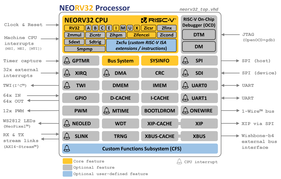
2. NEORV32 Processor (SoC)
The NEORV32 Processor provides a RISC-V-based full-scale microcontroller-like SoC platform build around the NEORV32 Central Processing Unit (CPU).
Section Structure
Key Features
-
optional SMP Dual-Core Configuration
-
optional internal bootloader (BOOTROM) with UART console & SPI/TWI flash and SD card boot options
-
optional RISC-V-compatible core local interruptor (CLINT)
-
optional two independent universal asynchronous receivers and transmitters (UART0, UART1) with optional hardware flow control (RTS/CTS)
-
optional serial peripheral interface host controller (SPI) with 8 dedicated CS lines
-
optional 8-bit serial data device interface (SDI)
-
optional two-wire serial interface controller (TWI), compatible to the I²C standard
-
optional two-wire serial device controller (TWD), compatible to the I²C standard
-
optional general purpose parallel IO port (GPIO), 32 inputs (interrupt capable), 32 outputs
-
optional 32-bit external bus interface, Wishbone-compatible (XBUS), AXI4-compatible bridge available
-
optional watchdog timer (WDT)
-
optional PWM controller with up to 32 individual channels (PWM)
-
optional ring-oscillator-based true random number generator (TRNG)
-
optional NeoPixel™/WS2812-compatible smart LED interface (NEOLED)
-
optional custom functions subsystem for custom co-processor extensions (CFS)
-
optional general purpose 32-bit timer (GPTMR) with up to 16 individual timer slices
-
optional 1-wire serial interface controller (ONEWIRE), compatible to the 1-wire standard
-
optional autonomous direct memory access controller (DMA)
-
optional stream link interface (SLINK), AXI4-Stream-compatible
-
optional on-chip debugger with JTAG TAP (OCD), optional authentication and hardware breakpoint
-
optional execution trace buffer to debug program flow (TRACER) via branch tracing
-
optional RVFI-compatible Execution Trace Port for advanced debugging, profiling and verification
-
optional system configuration information memory to determine hardware configuration via software (SYSINFO)
2.1. Processor Top Entity - Signals
The following table shows the interface signals of the processor top entity (rtl/core/neorv32_top.vhd).
All signals are of type std_ulogic or std_ulogic_vector, respectively. Custom interface type are used only
for the Execution Trace Port (trace_*).
|
Default Values of Inputs
All input signals - except for clock and reset - provide default values in case they are not explicitly assigned
during instantiation. The weak driver strengths of VHDL ('L' and 'H') are used to model a pull-down or pull-up
resistor for these unconnected inputs. After synthesis, these will result in 0 or 1, respectively.
|
|
Variable-Sized Ports
Some peripherals allow to configure the number of channels to-be-implemented by a generic (for example the number
of PWM channels). The according input/output signals have a fixed sized regardless of the actually configured
amount of channels. If less than the maximum number of channels is configured, only the LSB-aligned channels are used:
in case of an input port the remaining bits/channels are left unconnected; in case of an output port the remaining
bits/channels are hardwired to zero.
|
|
Tri-State Interfaces
Some interfaces (like the TWI, the TWD and the 1-Wire bus) require explicit tri-state drivers in the final top module.
|
|
Input/Output Registers
By default all output signals are driven by register and all input signals are synchronized into the processor’s
clock domain also using registers. However, for ASIC implementations it is recommended to add another register state
to all inputs and output so the synthesis tool can insert an explicit IO (boundary) scan chain.
|
| Name | Width | Direction | Default | Description |
|---|---|---|---|---|
Global Control (Processor Clocking and Processor Reset) |
||||
|
1 |
in |
none |
global clock line, all registers triggering on rising edge |
|
1 |
in |
none |
global reset, asynchronous, low-active |
|
1 |
out |
- |
On-Chip Debugger (OCD) reset output, synchronous, low-active |
|
1 |
out |
- |
Watchdog Timer (WDT) reset output, synchronous, low-active |
|
* |
out |
- |
CPU core 0 trace port (type |
|
* |
out |
- |
CPU core 1 trace port (type |
JTAG Access Port for On-Chip Debugger (OCD) |
||||
|
1 |
in |
|
serial clock |
|
1 |
in |
|
serial data input |
|
1 |
out |
- |
serial data output |
|
1 |
in |
|
mode select |
|
32 |
out |
- |
destination address |
|
32 |
out |
- |
read data |
|
3 |
out |
- |
cycle type |
|
3 |
out |
- |
access tag |
|
1 |
out |
- |
write enable ('0' = read transfer) |
|
4 |
out |
- |
byte enable |
|
1 |
out |
- |
strobe |
|
1 |
out |
- |
valid cycle |
|
32 |
in |
|
write data |
|
1 |
in |
|
transfer acknowledge |
|
1 |
in |
|
transfer error |
|
32 |
in |
|
RX data |
|
4 |
in |
|
RX source routing information |
|
1 |
in |
|
RX data valid |
|
1 |
in |
|
RX last element of stream |
|
1 |
out |
- |
RX ready to receive |
|
32 |
out |
- |
TX data |
|
4 |
out |
- |
TX destination routing information |
|
1 |
out |
- |
TX data valid |
|
1 |
out |
- |
TX last element of stream |
|
1 |
in |
|
TX allowed to send |
|
32 |
out |
- |
general purpose port direction control ( |
|
32 |
out |
- |
general purpose parallel output port |
|
32 |
in |
|
general purpose parallel input port (interrupt-capable) |
Primary Universal Asynchronous Receiver and Transmitter (UART0) |
||||
|
1 |
out |
- |
serial transmitter |
|
1 |
in |
|
serial receiver |
|
1 |
out |
- |
RX ready to receive new char |
|
1 |
in |
|
TX allowed to start sending, low-active |
Secondary Universal Asynchronous Receiver and Transmitter (UART1) |
||||
|
1 |
out |
- |
serial transmitter |
|
1 |
in |
|
serial receiver |
|
1 |
out |
- |
RX ready to receive new char |
|
1 |
in |
|
TX allowed to start sending, low-active |
|
1 |
out |
- |
controller clock line |
|
1 |
out |
- |
serial data output |
|
1 |
in |
|
serial data input |
|
8 |
out |
- |
select (low-active) |
|
1 |
in |
|
controller clock line |
|
1 |
out |
- |
serial data output |
|
1 |
in |
|
serial data input |
|
1 |
in |
|
chip select, low-active |
|
1 |
in |
|
serial data line sense input |
|
1 |
out |
- |
serial data line output (pull low only) |
|
1 |
in |
|
serial clock line sense input |
|
1 |
out |
- |
serial clock line output (pull low only) |
|
1 |
in |
|
serial data line sense input |
|
1 |
out |
- |
serial data line output (pull low only) |
|
1 |
in |
|
serial clock line sense input |
|
1 |
in |
|
1-wire bus sense input |
|
1 |
out |
- |
1-wire bus output (pull low only) |
|
16 |
out |
- |
pulse-width modulated channels |
|
256 |
in |
|
custom CFS input signal conduit |
|
256 |
out |
- |
custom CFS output signal conduit |
|
1 |
out |
- |
asynchronous serial data output |
|
64 |
out |
- |
CLINT.MTIMER system time output |
RISC-V Machine-Mode Processor Interrupts |
||||
|
1 |
in |
|
machine software interrupt (RISC-V), high-level-active; available only if CLINT is not enabled |
|
1 |
in |
|
machine timer interrupt (RISC-V), high-level-active; available only if CLINT is not enabled |
|
1 |
in |
|
machine external interrupt (RISC-V), high-level-active |
2.2. Processor Top Entity - Generics
This section lists all configuration generics of the NEORV32 processor top entity (rtl/neorv32_top.vhd).
These generics allow to configure the system according to your needs. The generics are
used to control implementation of certain CPU extensions and peripheral modules and even allow to
optimize the system for certain design goals like minimal area or maximum performance.
|
Default Values
All configuration generics provide default values in case they are not explicitly assigned during instantiation.
By default, all configuration options are disabled.
|
|
Software Discovery of Configuration
Software can determine the actual CPU configuration via the misa and mxisa[h] CSRs. The SoC/Processor configuration
can be determined via the SYSINFO memory-mapped registers.
|
| Name | Type | Default | Description |
|---|---|---|---|
General |
|||
|
natural |
0 |
The clock frequency of the processor’s |
|
boolean |
false |
Enable external CPU execution Execution Trace Port. |
|
boolean |
false |
Enable the SMP Dual-Core Configuration. |
|
natural |
0 |
Boot mode select; see Boot Configuration. |
|
suv(31:0) |
x"00000000" |
Custom CPU boot address (available if |
|
boolean |
false |
Implement the on-chip debugger and the CPU debug mode ( |
|
natural |
0 |
Number of implemented HW triggers (Trigger Module / |
|
boolean |
false |
Implement Debug Authentication module. |
|
suv(10:0) |
"00000000000" |
JEDEC ID: continuation codes plus vendor ID. |
|
boolean |
false |
Enable |
|
boolean |
false |
Enable |
|
boolean |
false |
Enable |
|
boolean |
false |
Enable |
|
boolean |
false |
Enable |
|
boolean |
false |
Enable |
|
boolean |
false |
Enable |
|
boolean |
false |
Enable |
|
boolean |
false |
Enable |
|
boolean |
false |
Enable |
|
boolean |
false |
Enable |
|
boolean |
false |
Enable |
|
boolean |
false |
Enable |
|
boolean |
false |
Enable |
|
boolean |
false |
Enable |
|
boolean |
false |
Enable |
|
boolean |
false |
Enable |
|
boolean |
false |
Enable |
|
boolean |
false |
Enable |
|
boolean |
false |
Enable |
|
boolean |
false |
Enable |
|
boolean |
false |
Enable |
|
boolean |
false |
Enable |
|
boolean |
false |
Enable |
|
boolean |
false |
Enable |
|
boolean |
false |
Enable |
|
boolean |
false |
Enable |
|
boolean |
false |
Enable |
|
boolean |
false |
Enable NEORV32-specific |
|
boolean |
false |
Implement constant-time branches (same execution times for taken and not-taken branches). |
|
boolean |
false |
Implement fast but large full-parallel multipliers (trying to infer DSP blocks); see section CPU Arithmetic Logic Unit. |
|
boolean |
false |
Implement fast but large full-parallel barrel shifters; see section CPU Arithmetic Logic Unit. |
|
natural |
0 |
CPU register file implementation style select; see section CPU Register File. |
Physical Memory Protection ( |
|||
|
natural |
0 |
Number of implemented PMP regions (0..16). |
|
natural |
4 |
Minimal region granularity in bytes. Has to be a power of two, min 4. |
|
boolean |
false |
Implement support for top-of-region (TOR) mode. |
|
boolean |
false |
Implement support for naturally-aligned power-of-two (NAPOT & NA4) modes. |
Hardware Performance Monitors ( |
|||
|
natural |
0 |
Number of implemented hardware performance monitor counters (0..29). |
|
natural |
64 |
Total LSB-aligned size of each HPM counter. Min 0, max 64. |
Internal Instruction Memory (IMEM) |
|||
|
boolean |
false |
Implement instruction memory. |
|
suv(31:0) |
x"00000000" |
Base address of the instruction memory (has to be naturally-aligned to its size). Handle with care. |
|
natural |
16*1024 |
Size in bytes of the instruction memory (use a power of 2). |
|
boolean |
false |
Add IMEM output register stage (improves mapping/timing at the expense of latency). |
Internal Data Memory (DMEM) |
|||
|
boolean |
false |
Implement data memory. |
|
suv(31:0) |
x"80000000" |
Base address of the data memory (has to be naturally-aligned to its size). Handle with care. |
|
natural |
8*1024 |
Size in bytes of the data memory (use a power of 2). |
|
boolean |
false |
Add DMEM output register stage (improves mapping/timing at the expense of latency). |
CPU Caches (Instruction Cache (iCache) & Data Cache (dCache)) |
|||
|
boolean |
false |
Implement the instruction cache ("I$"). |
|
natural |
4 |
Number of blocks ("lines"). Has to be a power of two. |
|
boolean |
false |
Implement the data cache ("D$") |
|
natural |
4 |
Number of blocks ("lines"). Has to be a power of two. |
|
natural |
64 |
global cache block size (I$ and D$) in bytes. Has to be a power of two, min 4. |
|
boolean |
true |
Enable burst transfers for cache updates. |
|
suv(31:0) |
x"F0000000" |
Base address of uncached address space. Has to be 256MB-aligned. |
Processor-External Bus Interface (XBUS) (Wishbone / AXI4-Compatible Bridging) |
|||
|
boolean |
false |
Implement the external bus interface. |
|
natural |
2048 |
Number of clock cycles after which an unacknowledged external bus access will auto-terminate (0 = disabled). |
|
boolean |
false |
Implement XBUS register stages to ease timing closure. |
|
natural |
0 |
Number of GPIO pairs, max 32. |
|
boolean |
false |
Enable optional GPIO direction control interface ( |
|
boolean |
false |
Implement CLINT. |
Primary Universal Asynchronous Receiver and Transmitter (UART0) |
|||
|
boolean |
false |
Implement UART0. |
|
natural |
1 |
UART0 RX FIFO depth, has to be a power of two, minimum value is 1, max 32768. |
|
natural |
1 |
UART0 TX FIFO depth, has to be a power of two, minimum value is 1, max 32768. |
Secondary Universal Asynchronous Receiver and Transmitter (UART1) |
|||
|
boolean |
false |
Implement UART1. |
|
natural |
1 |
UART1 RX FIFO depth, has to be a power of two, minimum value is 1, max 32768. |
|
natural |
1 |
UART1 TX FIFO depth, has to be a power of two, minimum value is 1, max 32768. |
|
boolean |
false |
Implement SPI controller. |
|
natural |
1 |
Depth of the SPI FIFO. Has to be a power of two, min 1, max 32768. |
|
boolean |
false |
Implement SDI controller. |
|
natural |
1 |
Depth of the SDI FIFO. Has to be a power of two, min 1, max 32768. |
|
boolean |
false |
Implement TWI controller. |
|
natural |
1 |
Depth of the TWI FIFO. Has to be a power of two, min 1, max 32768. |
|
boolean |
false |
Implement TWD controller. |
|
natural |
1 |
Depth of the TWD RX FIFO. Has to be a power of two, min 1, max 32768. |
|
natural |
1 |
Depth of the TWD TX FIFO. Has to be a power of two, min 1, max 32768. |
|
natural |
0 |
Number of PWM channels to implement (0..32). |
|
boolean |
false |
Implement WDT. |
|
boolean |
false |
Implement TRNG. |
|
natural |
1 |
Depth of the TRNG data FIFO. Has to be a power of two, min 1, max 32768. |
|
natural |
3 |
Total number of ring-oscillators. |
|
natural |
5 |
Number of inverters in first ring-oscillator; has to be odd. |
|
natural |
64 |
Number of raw random bits to process for one output byte; has to be power of 2. |
|
boolean |
false |
Implement CFS. |
|
boolean |
false |
Implement NEOLED controller. |
|
natural |
1 |
TX FIFO depth of the NEOLED controller. Has to be a power of two, min 1, max 32768. |
|
natural |
0 |
Number of individual GPTMR timer slices (0..16). |
|
boolean |
false |
Implement 1-wire controller. |
|
natural |
1 |
Depth of the 1-Wire FIFO. Has to be a power of two, min 1, max 32768. |
|
boolean |
false |
Implement DMA controller. |
|
natural |
4 |
Depth of the DMA transfer descriptor FIFO. Has to be a power of two, min 4, max 512. |
|
boolean |
false |
Implement stream link interface (AXI4-Stream-Compatible). |
|
natural |
1 |
SLINK RX FIFO depth, has to be a power of two, minimum value is 1, max 32768. |
|
natural |
1 |
SLINK TX FIFO depth, has to be a power of two, minimum value is 1, max 32768. |
|
boolean |
false |
Implement the trace buffer. |
|
natural |
1 |
Depth of the trace buffer. Has to be a power of two, min 1, max 32768. |
|
boolean |
false |
Write full trace log to file (simulation-only). |
2.3. Processor Clocking
The entire system is implemented as fully-synchronous logic design using a single clock domain that is driven
by the top’s clk_i signal. This clock signal is used by all internal registers and memories. All of them trigger
on the rising edge of this clock signal. External "clocks" like the OCD’s JTAG clock or the SDI’s serial clock
are synchronized into the processor’s clock domain before being used as "general logic signal" (and not as a dedicated clock).
2.3.1. Peripheral Clocks
Many processor modules like the UARTs or the timers provide a programmable time base for operations. In order to simplify
the hardware, the processor implements a global "clock generator" (neorv32_sys.vhd) that provides single-cycle clock enables
for certain frequencies which are derived from the main clock. These clock enable signals are synchronous to the system’s
main clock. The processor modules can use these enables for sub-main-clock operations while still providing a single
clock domain only.
In total, 8 sub-main-clock signals are available. All processor modules, which feature a time-based configuration, provide a
programmable three-bit prescaler select in their control register to select one of the 8 available clocks. The
mapping of the prescaler select bits to the according clock source is shown in the table below. Here, f represents the
processor main clock from the top entity’s clk_i signal.
Prescaler bits: |
|
|
|
|
|
|
|
|
Resulting clock: |
f/2 |
f/4 |
f/8 |
f/64 |
f/128 |
f/1024 |
f/2048 |
f/4096 |
2.4. Processor Reset
The NEORV32 processor includes a central reset sequencer (neorv32_sys.vhd) that handles all reset requests
and controls the internal reset nets. The processor-wide reset ("system reset") can be triggered by any
of the following sources:
-
the asynchronous low-active
rstn_itop entity input signal (external source) -
the On-Chip Debugger (OCD) (internal source)
-
the Watchdog Timer (WDT) (internal source)
|
Reset Cause
The actual reset cause can be determined via the Watchdog Timer (WDT).
|
If any of these sources triggers a reset, the internal system-wide reset will be active for at least 4 clock cycles ensuring
a valid reset of the entire processor. This system reset is asserted asynchronoulsy if triggered by the external
rstn_i signal and is asserted synchronously if triggered by an internal reset source. However, the system reset is
always de-asserted synchronously at the next rising clock edge.
Internally, all registers that are not meant for mapping to blockRAM (like the register file) do provide a dedicated and low-active asynchronous hardware reset. This asynchronous reset ensures that the entire processor logic is reset to a defined state even if the main clock is not operational yet.
2.5. Processor Interrupts
The system offers several interrupts (IRQs). Some can be used freely, others are reserved for specific tasks.
|
Trigger Type
All interrupt request lines are level-triggered and high-active. Once set, the signal should remain high until
the interrupt request is explicitly acknowledged (e.g. by writing to a memory-mapped register).
|
2.5.1. RISC-V Standard Interrupts
The processor supports the standard RISC-V machine-level interrupts for "machine timer interrupt (MTI)", "machine software interrupt (MSI)" and "machine external interrupt (MEI)". Their usage is defined by the RISC-V privileged architecture specification. See CPU section Traps, Exceptions and Interrupts for more information.
| Top signal | Description |
|---|---|
|
Machine software interrupt ( |
|
Machine timer interrupt ( |
|
Machine external interrupt ( |
2.5.2. NEORV32-Specific Fast Interrupt Requests
As part of the NEORV32-specific CPU extensions, the processor core features 16 fast interrupt request signals
(FIRQ0 to FIRQ15) with dedicated bits in mip and mie CSRs and custom mcause trap codes.
The FIRQ signals are reserved for processor-internal modules only (for example for the communication
interfaces to signal "available incoming data" or "ready to send new data").
The mapping of the 16 FIRQ channels to the according processor-internal modules is shown in the following table. The channel number also corresponds to the according FIRQ priority (0 = highest, 15 = lowest):
| Channel (priority) | Source |
|---|---|
0 |
reserved |
1 |
|
2 |
Primary Universal Asynchronous Receiver and Transmitter (UART0) |
3 |
Secondary Universal Asynchronous Receiver and Transmitter (UART1) |
4 |
|
5 |
|
6 |
|
7 |
|
8 |
|
9 |
|
10 |
|
11 |
|
12 |
|
13 |
|
14 |
|
15 |
2.6. Address Space
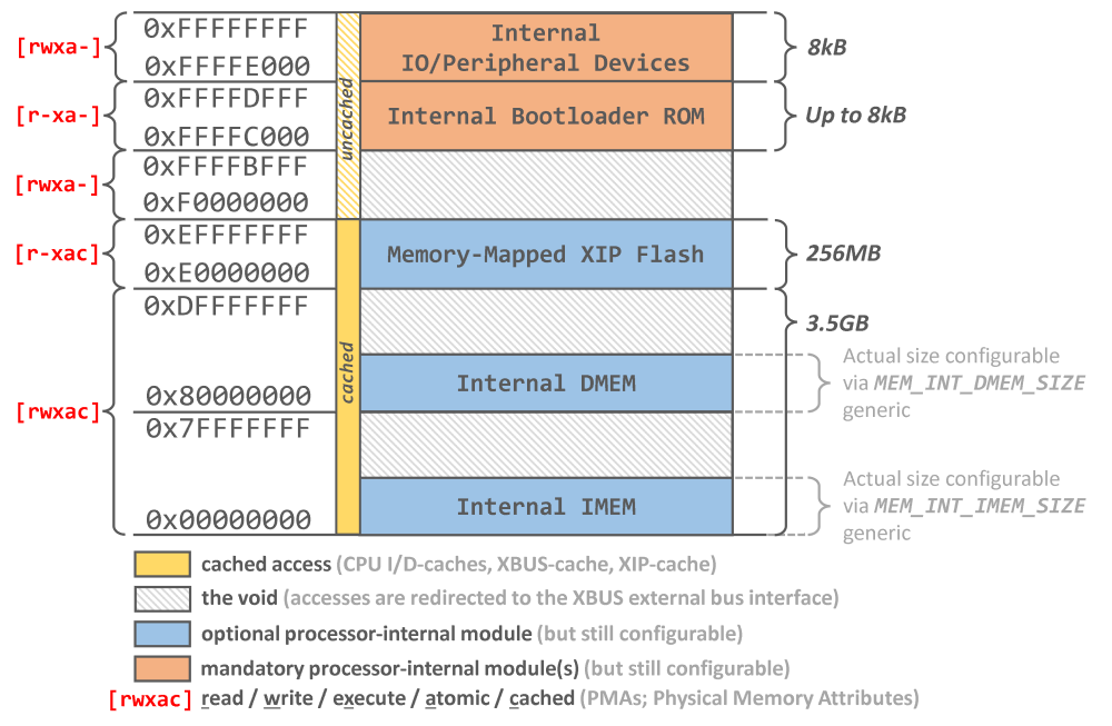
As a 32-bit architecture, NEORV32 can access up to 4GB of physical address space. The following figure shows the default address space layout with the according memory capabilites (physical memory attributes "PMAs"):
|
Custom Physical Memory Attributes
Custom physical memory attributes enforced by the CPU’s physical memory protection "PMP" (Smpmp ISA Extension)
can be used to further constrain the physical memory attributes.
|
The address space is highly configurable. Only the very last 2 MB (0xFFE00000 .. 0xFFFFFFFF) are exclusively reserved
for the NEORV32’s internal memory-mapped peripherals and I/O modules. The internal processor-internal Instruction Memory (IMEM)
and Data Memory (DMEM) (if enabled), on the other hand, can be mapped to any address via the configuration generics.
Accesses to "unmapped" addresses (a.k.a. the void) are redirected to the Processor-External Bus Interface (XBUS).
For example, if the processor-internal IMEM is disabled, accesses to the addresses starting at 0x00000000 (if not mapped
to the DMEM) are also redirected to the external bus interface. If the external bus interface is not enabled any access to
the void will raise a bus error exception.
By default, all addresses starting at 0xF0000000 are not cached by the CPU caches to provide direct access to memory-mapped
peripherals. However, this address boundary can be lowered by the according configuration generic (CACHE_UC_BASE) to
increase the size of the uncached address space. Note
|
Uncached Address Space
Please note that the uncached address space can only be altered in 256 MB increments. The uncached address space
starts at the configured 256 MB page and always extends to the end of the address space (0xFFFFFFFF).
|
2.6.1. Bus System
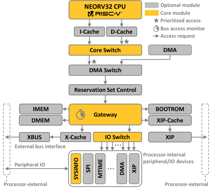
The CPU core provides individual interfaces for instruction fetch and data access. Both interface access the same address space making the core a von-Neumann architecture. Optionally, the two interface can be equipped with data and/or instruction caches (i-cache & d-cache).
The two CPU interfaces are multiplexed by a simple bus switch into a single processor-internal bus. Optionally, this bus is further multiplexed by another instance of the bus switch so the Direct Memory Access Controller (DMA) can also access the entire address space.
Accesses via the resulting SoC bus are routed by the Bus Gateway that is used to redirect the access to the processor-internal Instruction Memory (IMEM) (if implemented), the processor-internal Data Memory (DMEM) (if implemented), the processor-internal peripheral devices or - if the access does not target any of these - the Processor-External Bus Interface (XBUS). Accesses to the processor-internal IO/peripheral devices are further redirected via a dedicated IO Switch.
|
Bus System Infrastructure IP
The individual components of the processor’s bus system infrastructure are defined in rtl/core/neorv32_bus.vhd.
|
|
Bus Interface
See sections CPU Architecture and Bus Interface for more information regarding the CPU bus accesses
and the according protocol.
|
|
SMP Dual-Core Configuration
The dual-core configuration adds a second CPU core complex in parallel to the first one.
See section Dual-Core Configuration for more information.
|
2.6.2. Bus Gateway
The central bus gateway (VHDL component neorv32_bus_gateway) distributes CPU accesses to the two main memory
regions. Depending on the configuration, it routes accesses to:
-
Instruction Memory (IMEM) (if implemented)
-
Data Memory (DMEM) (if implemented)
-
processor-internal IO/peripherals
-
Processor-External Bus Interface (XBUS) (if implemented)
Additionally, the gateway also provides a bus monitor (aka "the bus keeper") that tracks all bus transactions to ensure safe and deterministic operations.
Bus Monitor and Timeout
For each single access the bus monitor starts an internal countdown.
The accessed module has to respond to the bus request within a bound time window. For processor-internal accesses
this time windows is defined by a constant in the main NEORV32 package file. For processor-external accesses
(via the external bus interface) this timeout is defined by the XBUS_TIMEOUT top configuration generic.
neorv32_package.vhd)constant int_bus_tmo_c : natural := 16; -- internal bus timeout window; has to be a power of twoneorv32_top.vhd)XBUS_TIMEOUT : natural := 2048; -- cycles after a pending bus access auto-terminates (0 = disabled)The according time window defines the maximum number of cycles after which a non-responding bus request will time out raising a bus access fault exception. For example this can happen when accessing "address space holes" - addresses that are not mapped to any physical module at all. The specific bus access exception type corresponds to the according access type (i.e. instruction fetch bus access fault, load bus access fault or store bus access fault).
2.6.3. IO Switch
The IO switch (VHDL component neorv32_bus_io_switch) decodes accesses to the procesor-internal IO/peripheral
address space. This 2MB address space is used to map all NEORV32 peripherals (like UART, SPI, timers, etc.),
the bootloader ROM and the on-chip debugger. Each device occupies an address range of 64kB; so up to 32 individual
devices can be mapped. The according address map is defined in the main VHDL package file (rtl/core/neorv32_package.vhd).
2.6.4. Atomic Memory Operations Controller
The CPU’s A ISA Extension adds support for atomic memory accesses. These atomic memory accesses are handles by
dedicated modules of the processor bus system. The SoC bus that is driven by the CPU core(s) is fed through two
atomic memory controller modules that handle read-modify-write operations as well as reservation-set operation:
| Hardware Module | CPU ISA Extensions | Description |
|---|---|---|
|
||
|
|
Direct/Non-Caches Atomic Accesses
Atomic operations always bypass the CPU’s data cache
using direct/uncached accesses. Care must be taken to maintain data Memory Coherence.
|
|
Physical Memory Attributes
Atomic memory operations can be executed targeting any address. This also includes
cached memory, memory-mapped IO devices and processor-external address spaces.
|
Atomic Read-Modify-Write Controller
This modules converts a single read-modify-write (RMW) memory operations request into two consecutive and atomic bus transactions. For each request, the controller executes an atomic set of three operations:
| Step | Pseudo Code | Description |
|---|---|---|
1 |
|
Perform a read operation from the targeted memory
address and temporarily store the loaded data into an internal buffer ( |
2 |
|
The buffered data from the first step is processed
using the write data provided by the CPU. The result is stored to another temporary internal buffer ( |
3 |
|
The data from the second buffer ( |
Atomic Reservation-Set Controller
In NEORV32 a reservation is defined by a 64-byte address granule that provides a guarding mechanism to support
atomic accesses (as specified by the RISC-V Zalrsc ISA Extension). A new reservation is registered by the
LR instruction. The address provided by this instruction defines the 64-byte-aligned memory region that is
monitored for exclusive accesses. The according SC instruction evaluates the state of this reservation. If the
reservation is still valid (same owner core / issueing core and same address granule) the write access performed by
the SC instruction is finally executed and the instruction returns a success state (i.e. rd = 0). If the
reservation has been invalidated or does not match, the SC instruction will not update main memory and will return
a failed state (i.e. rd = 1).
In either case, the SC instruction issues a downstream bus access to main memory (converted to a READ in case
of failure) to allow the detection of access faults for the target address also for failed SC instructions
which is required by the RISC-V specs.
|
The reservation-set controller implements a single reservation set per instance with a fixed granularity of 64 bytes.
Each reservation tracks the owning core’s ID and the aligned base address. A reservation is invalidated only when a
write access targets the same 64-byte address granule - read accesses, instruction fetches, and fence[.i] instructions
do not affect the reservation state.
The reservation-set controller is shared by both cores in the SMP Dual-Core Configuration. To ensure forward progress during concurrent atomic sequences, a turn-based arbitration mechanism is implemented:
-
An
LRinstruction can create (or update) a reservation if no reservation is active, if the requesting core already owns the current reservation, or if it is the requesting core’s "turn" (priority). -
A successful
SCflips the turn, ensuring that the other core receives priority for its nextLRattempt. -
A failed
SCfrom the owning core also clears the reservation, preventing stale reservations from blocking progress.
This guarantees atomic accesses and mutually exclusive access without starvation.
|
External Reservations
Note that the reservation-set controller cannot track memory accesses outside of the NEORV32 processor
(i.e. atomic accesses via the external bus interface) that are executed by processor-external agents.
|
2.6.5. Memory Coherence
Depending on the configuration, the NEORV32 memory hierarchy provides several levels/layers of memory.
-
The CPU execution pipeline and its instruction prefetch buffer (CPU Front-End)
-
The optional Data Cache (dCache) and Instruction Cache (iCache)
-
Processor-internal and processor-external memories (depending on setup configuration)
NEORV32 features up to three bus hosts: up to two CPU cores and the Direct Memory Access Controller (DMA). Since the levels of the memory hierarchy are transparent to the software, special care must be taken to ensure memory coherence is maintained throughout the entire system/application. Note that coherence and especially cache synchronization is not performed automatically by the hardware itself as there is no snooping implemented. NEORV32 supports two RISC-V memory ordering instructions that are used for manual memory synchronization:
-
fence: Flush the CPU’s data cache: modified ("dirty") blocks are copied back to main memory; all clean blocks are invalidated so that the next CPU access to any block results in a cache miss that reloads the cache with up-to-date data from main memory. -
fence.i: Perform the same operations asfence(i.e. flushing the data cache), but also clear the CPU’s instruction prefetch buffer and instruction cache. The next instruction cache access therefore results in a miss that fetches up-to-date data from main memory.
|
Weak Coherence Model
The NEORV32-specific implementation of the fence[.i] ordering instructions only provides a rather weak
coherence model. A core’s fence just orders all memory accesses towards main memory. Hence, they can become
visible by other agents (the secondary CPU core, the DMA, processor-external modules) if these agents also
synchronize (e.g. reload) their cache(s).
|
Atomic memory accesses also require special attention. All atomic memory accesses bypass the CPU caches. However, in this case, the caches explicitly ensure memory coherence. If the address of an atomic memory access is cached, the corresponding line is first written back to main memory if it has been modified. Afterward, the corresponding line is invalidated, and the atomic access is executed as a cache bypass. The next access to the atomic address bypasses the cache if it is again an atomic memory operation. Normal memory accesses result in a cache miss (since the corresponding line was automatically invalidated previously), so that the cache is reloaded with current data from main memory.
|
C-Language
Using plain _Atomic VariablesAtomic access (e.g., _Atomic int counter = 0;) defaults to GCC’s memory_order_seq_cst
builtin, which inserts fence instructions _before and after the access. This is the safest but slowest option.
|
2.7. Boot Configuration
The NEORV32 processor provides pre-defined boot configurations to adjust system start-up to
the requirements of the application. The actual boot configuration is defined by the BOOT_MODE_SELECT
generic (see Processor Top Entity - Generics).
For the SMP dual-core CPU configuration boot procedure see section Dual-Core Boot.
BOOT_MODE_SELECT |
Name | Boot address | Description |
|---|---|---|---|
0 (default) |
Bootloader |
Base of internal BOOTROM |
Implement the processor-internal Bootloader ROM (BOOTROM) as pre-initialized ROM and boot from there. |
1 |
Custom Address |
|
Start booting at user-defined address ( |
2 |
IMEM Image |
Base of internal IMEM |
Implement the processor-internal Instruction Memory (IMEM) as pre-initialized ROM and boot from there. |
2.7.1. Booting via Bootloader
This is the default configuration. When selected, the processor-internal Bootloader ROM (BOOTROM) is enabled.
This ROM contains the executable image (rtl/core/neorv32_bootrom_image.vhd) of the default NEORV32 Bootloader
that will be executed right after reset. The bootloader provides an interactive user console for executable upload as
well as an automatic mode to boot from external (SPI) flash memory.
If the processor-internal Instruction Memory (IMEM) is enabled it will be implemented as blank RAM.
2.7.2. Boot from Custom Address
This is the most flexible boot configuration as it allows the user to specify a custom boot address via the
BOOT_ADDR_CUSTOM generic. Note that this address has to be aligned to 4-byte boundary. The processor will
start executing from the defined address right after reset. For example, this boot configuration ca be used to
execute a custom bootloader from a memory that is attached via the Processor-External Bus Interface (XBUS).
For this configuration the processor-internal Bootloader ROM (BOOTROM) is not enabled / implement at all. If the processor-internal Instruction Memory (IMEM) is enabled it will be implemented as blank RAM.
2.7.3. Boot IMEM Image
This configuration will implement the Instruction Memory (IMEM) as pre-initialized ROM. The ROM is
initialized during synthesis with the according application image file (rtl/core/neorv32_imem_image.vhd).
After reset, the CPU will directly start executing this image. Since the IMEM is implemented as ROM, the
executable cannot be altered at runtime at all.
For this configuration the Bootloader ROM (BOOTROM) is not enabled / implement at all.
Note that this boot configuration requires the IMEM to be enabled (IMEM_EN = true).
|
Simulation Setup
This boot configuration is handy for simulations as the application software is executed right away without the
need for an explicit initialization / executable upload.
|
2.8. Processor-Internal Modules
|
Full-Word Write Accesses Only
Unless otherwise specified, all peripheral/IO devices should only be accessed using full-word accesses (i.e. 32-bit).
|
|
IO Module Address Space
Each peripheral/IO module occupies an address space of 64kB bytes. Most devices do not fully utilize this
address space and will mirror the available memory-mapped registers across the device’s address space.
However, only the specified memory-mapped registers addresses should be used.
|
|
Unimplemented Modules / Address Holes
When accessing an IO device that has not been implemented (disabled via the according generic)
or when accessing an address that is actually unused, a load/store access fault exception is raised.
|
|
Writing to Read-Only Registers
Unless otherwise specified, writing to registers that are listed as read-only does not trigger an exception
as the write access is just ignored by the corresponding hardware module.
|
|
Module Interrupts
Several peripheral/IO devices provide some kind of interrupt. These interrupts are mapped to the CPU’s
Custom Fast Interrupt Request Lines. See section Processor Interrupts for more information.
|
|
CMSIS System Description View (SVD)
A CMSIS-compatible System View Description (SVD) file including all peripherals is available in sw/svd.
|
2.8.1. Instruction Memory (IMEM)
Hardware source files: |
neorv32_imem.vhd |
generic processor-internal instruction memory (RAM or ROM) |
neorv32_imem_image.vhd |
memory initialization image (VHDL package) |
|
neorv32_imem_ram.vhd |
RAM component (primitive/IP wrapper) |
|
neorv32_imem_rom.vhd |
ROM component (primitive/IP wrapper) |
|
Software driver files: |
none |
|
Top entity ports: |
none |
|
Configuration generics: |
|
implement IMEM when |
|
32-bit base address (naturally aligned to IMEM size) |
|
|
IMEM size in bytes (use a power of 2) |
|
|
add IMEM output register stage |
|
|
implement IMEM as ROM when |
|
CPU interrupts: |
none |
Key Features
-
Burst-capable tightly-coupled on-chip instruction memory
-
Configurable RAM size
-
Accessible at the byte level
-
Mapped to memory primitives
-
Optional output register for improved timing
-
Can be implemented as pre-initialized ROM containing application firmware
Overview
Implementation of the processor-internal instruction memory is enabled by the processor’s
IMEM_EN generic. The total memory size in bytes is defined via the IMEM_SIZE generic.
Only sizes that are powers of two are supported. If enabled, the IMEM is mapped to base
address 0x00000000 by default (see section Address Space).
|
Custom IMEM Base Address
The base address of the IMEM can be customized via the IMEM_BASE generic. Please note that
the selected address must be naturally aligned to the IMEM size (IMEM_SIZE) and that there must
be no overlap with other sections of the internal Address Space (internal DMEM if enabled
and the internal IO/peripheral address space). Any non-default address must also be passed to the
Linker Script (e.g. USER_FLAGS += -Wl,--defsym,__neorv32_rom_base=<IMEM_BASE>).
|
By default the IMEM is implemented as true RAM so the content can be modified during run time.
Alternatively, the IMEM can be implemented as pre-initialized read-only memory (ROM), so the
processor can directly boot from it after reset. This option is configured via the BOOT_MODE_SELECT
generic. See section Boot Configuration for more information. If the IMEM is implemented as ROM
any write attempt to it will raise a store access fault exception.
The software framework provides an option to generate and override the default VHDL initialization
file rtl/core/neorv32_imem_image.vhd, which is automatically inserted into the IMEM (see
Makefile Targets. If the IMEM is implemented as RAM (default), the memory block will not be
initialized at all.
|
Output Register Stage
An optional output register stage can be enabled via IMEM_OUTREG_EN. For FPGA targets this might improve
mapping/timing results. Note that this option will increase the read latency by one clock cycle. Write accesses
are not affected by this at all.
|
|
Retrieve Memory Configuration by Software
Software can retrieve the DMEM size from the SYSINFO - Miscellaneous Configuration register.
|
|
Memory Primitives
The memory’s memory core is encapsulated as individual wrapper (neorv32_imem_ram.vhd / neorv32_imem_ram.vhd)
that can be replaced by a technology-specific IP. All interface ports provide static signal widths to ease replacement.
|
2.8.2. Data Memory (DMEM)
Hardware source files: |
neorv32_dmem.vhd |
generic processor-internal data memory (RAM) |
neorv32_dmem_ram.vhd |
RAM component (primitive/IP wrapper) |
|
Software driver files: |
none |
|
Top entity ports: |
none |
|
Configuration generics: |
|
implement DMEM when |
|
32-bit base address (naturally aligned to DMEM size) |
|
|
DMEM size in bytes (use a power of 2) |
|
|
add DMEM output register stage |
|
CPU interrupts: |
none |
Key Features
-
Burst-capable tightly-coupled on-chip data memory
-
Configurable RAM size
-
Accessible at the byte level
-
Can also be used for executing code
-
Mapped to memory primitives
-
Optional output register for improved timing
Overview
Implementation of the processor-internal data memory is enabled by the processor’s DMEM_EN
generic. The total memory size in bytes is defined via the DMEM_SIZE generic. Only sizes that
are powers of two are supported. If enabled, the DMEM is mapped to base address 0x80000000
by default (see section Address Space).
|
Custom DMEM Base Address
The base address of the DMEM can be customized via the DMEM_BASE generic. Please note that
the selected address must be naturally aligned to the DMEM size (DMEM_SIZE) and that there must
be no overlap with other sections of the internal Address Space (internal IMEM if enabled
and the internal IO/peripheral address space). Any non-default address must also be passed to the
Linker Script (e.g. USER_FLAGS += -Wl,--defsym,__neorv32_ram_base=<DMEM_BASE>).
|
|
Platform-Specific Memory Primitives
If required, the default DMEM can be replaced by a platform-/technology-specific primitive to
optimize area utilization, timing and power consumption.
|
|
Output Register Stage
An optional output register stage can be enabled via DMEM_OUTREG_EN. For FPGA targets this might improve
mapping/timing results. Note that this option will increase the read latency by one clock cycle. Write accesses
are not affected by this at all.
|
|
Retrieve Memory Configuration by Software
Software can retrieve the DMEM size from the SYSINFO - Miscellaneous Configuration register.
|
|
Memory Primitives
The memory’s memory core is encapsulated as individual wrapper (neorv32_dmem_ram.vhd) that can be
replaced by a technology-specific IP. All interface ports provide static signal widths to ease replacement.
|
2.8.3. Bootloader ROM (BOOTROM)
Hardware source files: |
neorv32_bootrom.vhd |
default platform-agnostic bootloader ROM |
neorv32_bootrom_image.vhd |
memory initialization image |
|
neorv32_bootrom_rom.vhd |
ROM component (primitive/IP wrapper) |
|
Software driver files: |
none |
implicitly used |
Top entity ports: |
none |
|
Configuration generics: |
|
implement BOOTROM when |
CPU interrupts: |
none |
Key Features
-
Tightly-coupled on-chip ROM
-
Accessible at the byte level
-
Mapped to memory primitives
-
Pre-initialized with default NEORV32 bootloader
Overview
The boot ROM contains the pre-compiled executable image of the default NEORV32 Bootloader. When the
Boot Configuration is set to bootloader mode (0) via the BOOT_MODE_SELECT generic, the
boot ROM is automatically enabled and the CPU boot address is adjusted to the base address of the boot ROM.
Note that the entire boot ROM is read-only.
|
Bootloader Image
The bootloader ROM is initialized during synthesis with the default bootloader image
(rtl/core/neorv32_bootrom_image.vhd). The physical size of the ROM is automatically
adjusted to the next power of two of the image size. However, note that the BOOTROM is
constrained to a maximum size of 64kB.
|
|
Memory Primitives
The memory’s memory core is encapsulated as individual wrapper (neorv32_bootrom_rom.vhd)
that can be replaced by a technology-specific IP. All interface ports provide static signal
widths to ease replacement.
|
2.8.4. Instruction Cache (iCache)
Hardware source files: |
neorv32_cache.vhd |
generic cache module |
neorv32_cache_ram.vhd |
tag and data RAM (primitive/IP wrapper) |
|
Software driver files: |
none |
|
Top entity ports: |
none |
|
Configuration generics: |
|
implement CPU-exclusive instruction cache (I$) when |
|
number of cache blocks ("cache lines"); has to be a power of two |
|
|
size of a cache block in bytes (global configuration for I$ and D$); has to be a power of two, min 4 |
|
|
enable burst transfers for cache update |
|
|
base address of uncached address space; has to be 256MB-aligned |
|
CPU interrupts: |
none |
Key Features
-
Direct-mapped read-only cache
-
Configurable number of lines
-
Configurable line size
-
Allows bypassing for uncached accesses
-
Tag and data RAM mapped to memory primitives
Overview
The processor features an optional instruction cache (i-cache) that is directly connected to the CPU Front-End instruction fetch interface providing full-transparent accesses. The cache is direct-mapped and read-only. For the Dual-Core Configuration each CPU core is equipped with a private instruction cache.
The instruction cache is enabled by the ICACHE_EN generic. The total cache memory size in bytes is defined
by ICACHE_NUM_BLOCKS x CACHE_BLOCK_SIZE. ICACHE_NUM_BLOCKS defines the number of cache blocks ("lines")
and CACHE_BLOCK_SIZE defines the block (line) size in bytes; note that the latter configuration is global
for all caches.
|
Retrieve Cache Configuration by Software
Software can retrieve the cache configuration/layout from the SYSINFO - Cache Configuration register.
|
|
Memory Primitives
The cache’s tag and data RAMs are encapsulated as wrapper (neorv32_cache_ram.vhd) that can be modified or
replaced by a technology-specific IP. All interface ports provide static signal widths to ease replacement.
|
Burst Transfers
Cache update operations can use burst transfers to increase performance.
Burst operations are enabled (for all caches) by the CACHE_BURSTS_EN top generic. When bursts are enabled
all cache block transfers are always executed as burst transfers. Hence, all devices, memories and endpoints
that can be accessed by the cache must also be able to process bursts (including modules connected to the
Processor-External Bus Interface (XBUS)).
Cache Bypass
The cache provides direct/uncached accesses (bypassing the cache) in order to access memory-mapped peripherals.
The base adress of the uncached address space is configured by the CACHE_UC_BASE generic. Note that only the
4 MSBs of this address are evaluated resulting in a 256MB granulrity. All accesses that target the address range
from CACHE_UC_BASE to 0xFFFFFFFF will bypass the cache. See section Address Space for more information.
Cache Synchronization and Memory Coherence
By executing the fence.i instruction the entire i-cache is invalidated. The next access therefore results
in a cache miss that reloads the cache with up-to-date data from main memory. See section
Memory Coherence for more information.
Cache Bus Error Handling
The cache responds differently to bus errors depending on which operation caused the error. Note that all instruction cache accesses are entirely read-only.
-
Cache Bypass: If a bus error occurs during a cache bypass operation - for example, when accessing memory-mapped I/O - the bus error is reported to the CPU immediately and with full precision. The address reported in
mepcrepresents the exact address that caused the error. -
Cache Miss: If the instruction request results in a cache miss, the according memory block is fetched from main memory. If any memory access within this block transfer causes a bus error, the entire cache block is discarded and the bus error is reported to the CPU immediately and with partial precision. The address reported in
mepcrepresents an address within the cache/memory block whose fetch caused the error. -
Cache Synchronization: A cache synchronization operation (
fence.i) cannot cause any bus error as it just invalided all current cache blocks without performing any memory access at all.
2.8.5. Data Cache (dCache)
Hardware source files: |
neorv32_cache.vhd |
generic cache module |
neorv32_cache_ram.vhd |
tag and data RAM (primitive/IP wrapper) |
|
Software driver files: |
none |
|
Top entity ports: |
none |
|
Configuration generics: |
|
implement CPU-exclusive data cache (D$) when |
|
number of cache blocks ("cache lines"); has to be a power of two |
|
|
size of a cache block in bytes (global configuration for I$ and D$); has to be a power of two, min 4 |
|
|
enable burst transfers for cache update |
|
|
base address of uncached address space; has to be 256MB-aligned |
|
CPU interrupts: |
none |
Key Features
-
Direct-mapped cache with write-back & write-allocated write policies
-
Configurable number of lines
-
Configurable line size
-
Allows bypassing for uncached accesses
-
Tag and data RAM mapped to memory primitives
Overview
The processor features an optional data cache (d-cache) that is directly connected to the CPU Load/Store Unit data interface providing full-transparent accesses. The cache is direct-mapped and uses write-back (copy modified cache lines back to main memory when evicted) and write-allocate (fetch entire line on a write-miss) write policies. For the Dual-Core Configuration each CPU core is equipped with a private data cache.
The data cache is enabled by the DCACHE_EN generic. The total cache memory size in bytes is defined by
DCACHE_NUM_BLOCKS x CACHE_BLOCK_SIZE. DCACHE_NUM_BLOCKS defines the number of cache blocks ("lines")
and CACHE_BLOCK_SIZE defines the block (line) size in bytes; note that the latter configuration is global
for all caches.
|
Retrieve Cache Configuration by Software
Software can retrieve the cache configuration/layout from the SYSINFO - Cache Configuration register.
|
|
Memory Primitives
The cache’s tag and data RAM is encapsulated as individual wrapper (neorv32_cache_ram.vhd) that can be
replaced by a technology-specific IP. All interface ports provide static signal widths to ease replacement.
|
Burst Transfers
Cache update operations can use burst transfers to increase performance.
Burst operations are enabled (for all caches) by the CACHE_BURSTS_EN top generic. When bursts are enabled
all cache block transfers are always executed as burst transfers. Hence, all devices, memories and endpoints
that can be accessed by the cache must also be able to process bursts (including modules connected to the
Processor-External Bus Interface (XBUS)).
Cache Bypass
The cache provides direct/uncached accesses (bypassing the cache) in order to access memory-mapped peripherals.
The base adress of the uncached address space is configured by the CACHE_UC_BASE generic. Note that only the
4 MSBs of this address are evaluated resulting in a 256MB granulrity. All accesses that target the address range
from CACHE_UC_BASE to 0xFFFFFFFF will bypass the cache. See section Address Space for more information.
All atomic memory accesses also bypass the cache regardless of the adress; however, in this case, the cache explicitly ensures Memory Coherence: if the address of an atomic memory access is cached, the corresponding line is first written back to main memory if it has been modified. The corresponding line is then invalidated, and the atomic access is finally executed as a cache-bypassing access.
Cache Synchronization and Memory Coherence
By executing the fence instruction the data cache is flushed: modified ("dirty") blocks are copied back to main
memory; all clean blocks are invalidated so that the next CPU access to any block results in a cache miss that
reloads the cache with up-to-date data from main memory. See section Memory Coherence for more information.
Cache Bus Error Handling
The cache responds differently to bus errors depending on which operation caused the error.
-
Cache Bypass: If a bus error occurs during a cache bypass operation - for example, when accessing memory-mapped I/O - the bus error is reported to the CPU immediately and with full precision. The address reported in
mtvalrepresents the exact address that caused the error. -
Cache Miss Without Eviction: If the CPU request results in a cache miss that can be completed without, the according memory block is fetched from main memory. If any memory access within this block transfer causes a bus error, the entire cache block is discarded and the bus error is reported to the CPU immediately and with partial precision. The address reported in
mtvalrepresents an address within the cache/memory block whose fetch caused the error. -
Cache Miss With Eviction: If the CPU request results in a cache miss that requires the write-back of a modified ("dirty") cache block, the modified is copied back to main memory before fetching the actual requested memory block. If this write-back causes any buss error, the modified cache block being written back is discarded and the bus error is reported to the CPU immediately and imprecisley. The address reported in
mtvalonly represents an address inside the requested memory block - not an address within the block that the cache was trying to write back.
|
Bus-Errors During Cache Write-Back
This type of cache-related "background" bus error is difficult to debug and - like most other bus errors - might
be fatal when occurring in machine mode. A future version of NEORV32 will include an improved mechanism for
determining the exact address of this type of bus error.
|
-
Cache Synchronization: If the cache encounters a bus error while writing modified cache blocks back to main memory during a cache synchronization operation (
fence), the cache block that caused the error is remains valid but also "dirty" (not sync with main memory). The next CPU access that results in a cache miss with eviction of this block will encounter a bus error that is reported to the CPU immediately and imprecisley (see above).
2.8.6. Direct Memory Access Controller (DMA)
Hardware source files: |
neorv32_dma.vhd |
|
Software driver files: |
neorv32_dma.c |
|
neorv32_dma.h |
||
Top entity ports: |
none |
|
Configuration generics: |
|
implement DMA when |
|
descriptor FIFO depth, has to be a power of 2, min 4, max 512 |
|
CPU interrupts: |
fast IRQ channel 10 |
DMA transfer(s) done (see Processor Interrupts) |
Key Features
-
CPU-independent data movement
-
Byte-wide or word-wide data transfers
-
Up to 16MB (bytes) or 64MB (words) per transfer
-
Optional Endianness conversion
-
Optional descriptor FIFO
-
Chaining of pre-programmed transfers
-
Transfer-done interrupt
Overview
The NEORV32 DMA features a lightweight direct memory access controller that allows to move and modify data independently of the CPU. Only a single read/write channel is implemented. So only one programmed transfer can be in progress at a time. However, a configurable descriptor FIFO is provided which allows to program several transfers so the DMA can execute them one after the other.
The DMA is connected to the central processor-internal bus system (see section Address Space) and can access the entire/same address space as the CPU core. It uses interleaving mode accessing the central processor bus only if the CPU does not currently request a bus access. The DMA controller can handle different data quantities (e.g. read bytes and write them back as zero-extended words) and can also change the Endianness of data while transferring. It supports reading/writing data from/to fixed or auto-incrementing addresses.
|
DMA Bus Access
Transactions performed by the DMA are executed as bus transactions with elevated machine-mode privilege level.
Note that any physical memory protection rules (Smpmp ISA Extension) are not applied to DMA transfers.
Furthermore, the DMA uses single-transfers only (.e. no burst transfers).
|
|
DMA Demo Program
A DMA example program can be found in sw/example/demo_dma.
|
Theory of Operation
The DMA provides just two memory-mapped interface registers: A status and control register CTRL and
another one for writing the transfer descriptor(s) to the internal descriptor FIFO.
The DMA is enabled by setting the DMA_CTRL_EN bit of the control register. Clearing this flag will abort any outstanding
transfer and will also reset/clear the descriptor FIFO. A programmed DMA transfer is initiated by setting the control
register’s DMA_CTRL_START bit. Setting this bit while the descriptor FIFO is empty has no effect. The current status
of the FIFO can be checked via the DMA_CTRL_D* flags.
The DMA uses an atomic read-modify-write transfer process. Data is read from the current source address, modified/aligned
internally and then written back to the current destination address. If the DMA controller encounters a bus error during
operation, it will set the DMA_CTRL_ERROR flag and will terminate the current transfer. An new transfer can only start
if the DMA_CTRL_ERROR flag is cleared manually.
When the DMA_CTRL_DONE flag is set the DMA has completed all programmed transfers, i.e. all descriptors from the FIFO
were executed. This flag also triggers the DMA controller’s interrupt request signal. The application software has to
clear DMA_CTRL_DONE in order to acknowledge the interrupt and to start further transfers.
DMA Descriptor
All DMA transfers are executed based on descriptors. A descriptor contains the data source and destination base addresses as well as the number of elements to transfer and the data type and handling configuration. A complete descriptor is encoded as 3 consecutive 32-bit words:
| Index | Size | Description |
|---|---|---|
0 |
32-bit |
Source data base address |
1 |
32-bit |
Destination data base address |
2 |
32-bit |
Transfer configuration word (see next table) |
|
Descriptor FIFO Size
The descriptor FIFO has a minimal size of 4 entries. This can be extended by the IO_DMA_DSC_FIFO generic.
|
|
Incomplete Descriptors
The DMA controller consumes 3 entries from the FIFO for each transfer. If the FIFO does not provide a complete
DMA descriptor, the controller will wait until a complete descriptor is available.
|
The source and destination data addresses can target any memory location in the entire 32-bit address space including memory-mapped peripherals. The number of elements to transfer as well as incrementing or constant byte- or word-level transfers are configured via the transfer configuration word (3rd descriptor word):
| Bit(s) | Name | Description |
|---|---|---|
|
|
Number of elements to transfer; must be greater than zero |
|
- |
reserved, set to zero |
|
|
Set to swap byte order ("Endianness" conversion) |
|
|
Source data configuration (see list below) |
|
|
Destination data configuration (see list below) |
Source and destination data accesses are configured by a 2-bit selector individually for the source and the destination data:
-
00: Constant byte - transfer data as byte (8-bit); do not alter address during transfer -
01: Constant word - transfer data as word (32-bit); do not alter address during transfer -
10: Incrementing byte - transfer data as byte (8-bit); increment the source address by 1 -
11: Incrementing word - transfer data as word (32-bit); increment the source address by 4
Optionally, the controller can automatically swap the logical byte order ("Endianness") of the transferred data
when the DMA_CONF_BSWAP bit is set.
Register Map
| Address | Name [C] | Bit(s), Name [C] | R/W | Function |
|---|---|---|---|---|
|
|
|
r/w |
DMA module enable; reset module when cleared |
|
-/w |
Start programmed DMA transfer(s) |
||
|
r/- |
reserved, read as zero |
||
|
r/- |
Descriptor FIFO depth, log2( |
||
|
r/- |
reserved, read as zero |
||
|
-/w |
Write |
||
|
r/- |
Descriptor FIFO is empty |
||
|
r/- |
Descriptor FIFO is full |
||
|
r/- |
Bus access error during transfer or incomplete descriptor data |
||
|
r/1 |
All transfers executed |
||
|
r/- |
DMA transfer(s) in progress |
||
|
|
|
-/w |
Descriptor FIFO write access |
2.8.7. Processor-External Bus Interface (XBUS)
Hardware source files: |
neorv32_xbus.vhd |
External bus gateway |
Software driver files: |
none |
|
Top entity ports: |
|
address output (32-bit) |
|
data input (32-bit) |
|
|
data output (32-bit) |
|
|
cycle type (3-bit) |
|
|
access tag (3-bit) |
|
|
write enable (1-bit) |
|
|
byte enable (4-bit) |
|
|
bus strobe (1-bit) |
|
|
valid cycle (1-bit) |
|
|
acknowledge (1-bit) |
|
|
bus error (1-bit) |
|
Configuration generics: |
|
enable external bus interface when |
|
number of clock cycles after which an unacknowledged external bus access will auto-terminate (0 = disabled) |
|
|
implement XBUS register stages |
|
( |
burst size (defined by global cache block size) |
|
( |
enable burst transfers for cache update |
|
CPU interrupts: |
none |
Key Features
-
Gateway for processor-external modules
-
Wishbone-compatible bus protocol
-
Optional burst support
-
Optional AXI4-compatible bridging
Overview
The external bus interface provides a Wishbone-compatible on-chip bus interface. This bus interface can be used to attach processor-external modules like memories, custom hardware accelerators or additional peripheral devices.
|
Burst Transfers
If any cache (i-cache or d-cache)
is implemented and bursts are globally enabled (by the CACHE_BURSTS_EN top generic) all cache block transfers are
always executed as burst transfers with a burst size equal to the cache block size (CACHE_BLOCK_SIZE top generic).
Burst transfers should not be enabled if any external module mapped to cached Address Space does not support bursts.
Note that burst transactions need to set ACK or ERR for each burst element. Note that the cycle type identifier signal
(xbus_cti_o) does not support the end-of-burst identifier.
|
|
Address Mapping
The external interface is not mapped to a specific address range. Instead, all CPU memory accesses that
do not target a specific (and actually implemented) processor-internal address region (hence, accessing the "void";
see section Address Space) are redirected to the external bus interface.
|
|
Wishbone Specs
The official Wishbone specification scan be found online:
https://wishbone-interconnect.readthedocs.io/en/latest/index.html
|
|
AXI4-Compatible Interface Bridge
A bridge that converts the processor’s XBUS interface into an AXI4-compatible host interface is available
in rtl/system_integration/xbus2axi4_bridge.vhd. This bridge is also used for the ENORV32 Vivado IP block:
https://stnolting.github.io/neorv32/ug/#_packaging_the_processor_as_vivado_ip_block
|
XBUS Bus Protocol
The external bus interface implements a subset of the pipelined Wishbone protocol.
Basically, three types of bus transfer are implemented which are illustrated in the following figures.
The actual transfer type is indicated via the cycle type identifier (xbus_cti_o) signal.
-
Single-access (
xbus_cti_o = 000) transfers perform a single read or write operation. -
Atomic-access (
xbus_cti_o = 001) transfers perform a read followed by a write operation. The bus is locked during the entire transfer (keepingcychigh) to maintain exclusive bus access. This transfer type is used by the CPU to perform atomic read-modify-write operations. -
Burst read (
xbus_cti_o = 010) transfers perform several consecutive read accesses. This transfer type is used by cache block operations.
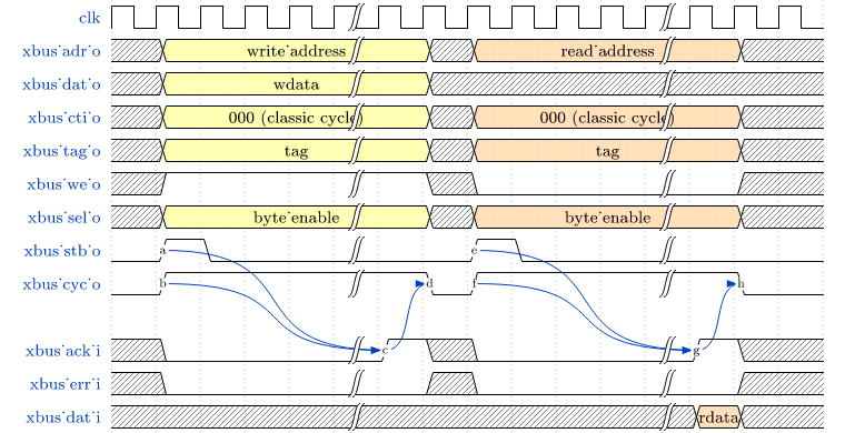
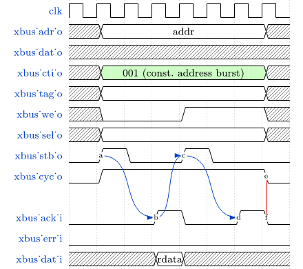
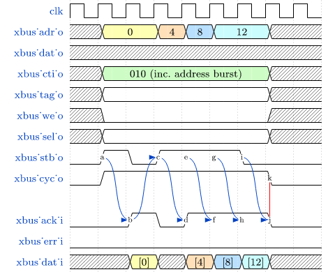
Bus Latency
An accessed XBUS device does not have to respond immediately to a bus request by sending an ACK.
Instead, there is a time window where the device has to acknowledge the transfer. This time window
is configured by the XBUS_TIMEOUT generic. Note that the value provided by this generic is internally
extended to the next power of two.
All XBUS transactions have to be acknowledged within this time window. Otherwise the transfer is terminated and a bus fault exception is raised. See section Bus Monitor and Timeout for more information.
Furthermore, an accesses XBUS device can signal an error condition at any time by setting the ERR signal
high for one cycle. This will also terminate the current bus transaction raising a CPU bus fault exception.
|
Register Stage
An optional register stage can be added to the XBUS gateway to break up the critical path easing timing closure.
When XBUS_REGSTAGE_EN is true all outgoing and incoming XBUS signals are registered increasing access latency
by two cycles. Furthermore, all outgoing signals (like the address) will be kept stable if there is no bus access
being initiated.
|
Access Tag
The XBUS tag signal xbus_tag_o provides additional information about the current access cycle.
The encoding is compatible to the AXI4 xPROT signal.
-
xbus_tag_o(2)I: access is an instruction fetch when set; access is a data access when cleared -
xbus_tag_o(1)NS: this bit is hardwired to0indicating a secure access -
xbus_tag_o(0)P: access is performed from privileged mode (machine-mode) when set
2.8.8. Stream Link Interface (SLINK)
Hardware source files: |
neorv32_slink.vhd |
|
Software driver files: |
neorv32_slink.c |
|
neorv32_slink.h |
||
Top entity ports: |
|
RX link data (32-bit) |
|
RX routing information (4-bit, optional) |
|
|
RX link data valid (1-bit) |
|
|
RX link last element of stream (1-bit, optional) |
|
|
RX link ready to receive (1-bit) |
|
|
TX link data (32-bit) |
|
|
TX routing information (4-bit, optional) |
|
|
TX link data valid (1-bit) |
|
|
TX link last element of stream (1-bit, optional) |
|
|
TX link allowed to send (1-bit) |
|
Configuration generics: |
|
implement SLINK when true |
|
RX FIFO depth, has to be a power of two, min 1 |
|
|
TX FIFO depth, has to be a power of two, min 1 |
|
CPU interrupts: |
fast IRQ channel 14 |
SLINK IRQ (see Processor Interrupts) |
Key Features
-
Compatible to the AXI-4 stream standard
-
Independent RX and TX channels
-
Optional per-channel FIFOs
-
Supports "last" and "source/destination" stream signals
-
Interrupt based on FIFO status
Overview
The stream link interface provides independent RX and TX channels for sending and receiving stream data.
Each channel features a configurable internal data FIFO (IO_SLINK_RX_FIFO and IO_SLINK_TX_FIFO). The
SLINK interface provides higher bandwidth and less latency than the external bus interface making it
ideally suited for coupling custom stream processors or streaming peripherals.
|
Example Program
An example program for the SLINK module is available in sw/example/demo_slink.
|
Interface & Protocol
Each link/channel consists of the following signals:
-
datprovides the actual data word -
valindicates the current transmission cycle is valid -
lstindicates the current transmission cycle is the last element of a stream (optional) -
rdyindicates the receiver is ready to receive -
srcanddstprovide source/destination routing information (optional)
|
AXI4-Stream Compatibility
The interface names (except for src and dst) and the underlying protocol is compatible to the AXI4-Stream
protocol standard. A processor top entity with AXI4-Stream-compatible interfaces can be found in
rtl/system_inegration. More information can be found in the user guide:
https://stnolting.github.io/neorv32/ug/#_packaging_the_processor_as_vivado_ip_block
|
Theory of Operation
The SLINK provides four interface register. The control register (CTRL) is used to configure the module and to
check its status. The ROUTE register can be used to configure a 4-bit routing ID. Two individual data registers
(DATA and DATA_LAST) are used to send and receive the actual data.
The DATA register provides direct access to the RX/TX FIFO buffers. Read accesses return data from the RX FIFO.
The end-of-stream delimiter as well as the RX routing information are also buffered in the RX FIFO and can be obtained
from control register’s SLINK_CTRL_RX_LAST flag and the ROUTE register, respectively, after reading the actual RX data.
Writing to the DATA register will immediately write to the TX link FIFO. Writing to the DATA_LAST register will
also push data to the TX link FIFO and will also set the end-of-stream delimiter for that data word. TX routing
information can be configured via the ROUTE register before writing data to DATA / DATA_LAST.
The configured FIFO sizes can be retrieved by software via the control register’s SLINK_CTRL_RX_FIFO_* and
SLINK_CTRL_TX_FIFO_* bits.
The SLINK is globally enabled by setting the control register’s enable bit SLINK_CTRL_EN. Clearing this bit will
reset all internal logic and will also clear both FIFOs. Writing to the TX channel’s FIFO while it is full will
have no effect. Reading from the RX channel’s FIFO while it is empty will also have no effect and will return
the last received data word. The current status of the RX and TX FIFOs can be determined via the control register’s
SLINK_CTRL_RX_EMPTY, SLINK_CTRL_RX_FULL, SLINK_CTRL_TX_EMPTY and SLINK_CTRL_TX_FULL flags.
Interrupt
The SLINK module provides a single interrupt request that can be used to signal certain RX/TX data FIFO conditions.
The interrupt conditions are based on the RX/TX FIFO status flags SLINK_CTRL_RX_* / SLINK_CTRL_TX_* and are
configured via the according SLINK_CTRL_IRQ_RX_* / SLINK_CTRL_IRQ_TX_* bits. The SLINK interrupt will fire when the
module is enabled (SLINK_CTRL_EN) and any of the enabled interrupt conditions is met. Hence, all enabled interrupt
conditions are logically OR-ed. The interrupt remains active until all interrupt-causing conditions are resolved.
Register Map
| Address | Name [C] | Bit(s) | R/W | Function |
|---|---|---|---|---|
|
|
|
r/w |
SLINK global enable |
|
r/- |
reserved, read as zero |
||
|
r/- |
RX FIFO empty |
||
|
r/- |
RX FIFO full |
||
|
r/- |
TX FIFO empty |
||
|
r/- |
TX FIFO full |
||
|
r/- |
Last word read from |
||
|
r/- |
reserved, read as zero |
||
|
r/w |
Fire interrupt if RX FIFO not empty |
||
|
r/w |
Fire interrupt if RX FIFO full |
||
|
r/w |
Fire interrupt if TX FIFO empty |
||
|
r/w |
Fire interrupt if TX FIFO not full |
||
|
r/- |
reserved, read as zero |
||
|
r/- |
log2(RX FIFO size) |
||
|
r/- |
log2(TX FIFO size) |
||
|
|
|
-/w |
TX destination routing information ( |
|
r/- |
RX source routing information ( |
||
|
r/- |
reserved, read as zero |
||
|
|
|
r/w |
Write data to TX FIFO; read data from RX FIFO |
|
|
|
r/w |
Write data to TX FIFO (and also set end-of-stream delimiter); read data from RX FIFO |
2.8.9. General Purpose Input and Output Port (GPIO)
Hardware source files: |
neorv32_gpio.vhd |
|
Software driver files: |
neorv32_gpio.c |
|
neorv32_gpio.h |
||
Top entity ports: |
|
32-bit direction control output port |
|
32-bit parallel output port |
|
|
32-bit parallel input port |
|
Configuration generics: |
|
number of input/output pairs to implement (0..32) |
|
enable direction control feature when true |
|
CPU interrupts: |
fast IRQ channel 8 |
input-pin change interrupt (see Processor Interrupts) |
Key Features
-
Up to 32 inputs and 32 outputs
-
Each input pin is interrupt-capable
-
Configurable interrupt triggers (positive/negative level or edge)
Overview
The general purpose IO module provides simple unidirectional - or optionally bidirectional - inputs and outputs. These connections can be used externally (for example, to control status LEDs, connect buttons, etc.) or internally to provide control signals for other IP modules. The input port features programmable, pin-specific level- or edge-triggered interrupts.
Data written to the PORT_OUT will appear on the processor’s gpio_o port. Vice versa, the PORT_IN register
represents the current state of the processor’s gpio_i.
The actual number of input/output pairs is defined by the IO_GPIO_NUM generic. When set to zero, the GPIO module
is excluded from synthesis and the output port gpio_o is tied to all-zero. If IO_GPIO_NUM is less than the
maximum value of 32, only the LSB-aligned bits of gpio_o and gpio_i are actually connected while the remaining
ones are tied to zero or are left unconnected, respectively. This also applies to all memory-mapped interface
registers of the GPIO module (i.e. the according most-significant bits are hardwired to zero and are read-only).
Direction Control
The IO ports can also be used as bidirectional ports. The direction feature must be explicitly enabled via the
IO_GPIO_DIR_EN generic. When enabled, the PORT_DIR register is used to control the direction of each individual
IO signal by directly driving the top’s gpio_dir_o port. Setting bit i to 1 configures the according pin as
output. Clearing bit i configures the according pin as input. Note that the PORT_DIR register resets to all-zero
configuring all bi-directional IOs as inputs.
gpio_dir_o[i] -------+    0 = input (default)
                     |    1 = output
                   |\|
                   | \
gpio_o[i] -------->|  >---+---<> GPIO pin [i]
                   | /    |
                   |/     |
                          |
gpio_i[i] <---------------+
gpio_io port is of type std_logic_vector)gpio_tristate_gen:
for i in 0 to IO_GPIO_NUM-1 generate
gpio_io(i) <= std_logic(gpio_o(i)) when (gpio_dir_o(i) = '1') else 'Z'; -- drive
end generate;
gpio_i(IO_GPIO_NUM-1 downto 0) <= std_ulogic_vector(gpio_io(IO_GPIO_NUM-1 downto 0)); -- sense
GPIO_DIR As Additional Output Portgpio_dir_o port can be used as additional output port.
|
Interrupts
Each input pin (gpio_i) provides an individual programmable interrupt trigger. The actual interrupt trigger
type can be configured individually for each input pin using the IRQ_TYPE and IRQ_POLARITY registers.
IRQ_TYPE defines the actual trigger type (level-triggered or edge-triggered), while IRQ_POLARITY defines
the trigger’s polarity (low-level/falling-edge or high-level/rising-edge). The position of each bit in these
registers corresponds the according gpio_i input pin.
Each pin interrupt channel can be enabled or disabled individually using the IRQ_ENABLE register. Each bit
in this register corresponds to the according input pin. If the programmed trigger of a disabled input
(IRQ_ENABLE(i) = 0) fires, the interrupt request is entirely ignored.
IRQ_ENABLE(i) |
IRQ_TYPE(i) |
IRQ_POLARITY(i) |
Resulting trigger of gpio_i(i) |
|---|---|---|---|
|
|
|
low-level ( |
|
|
|
high-level ( |
|
|
|
falling-edge ( |
|
|
|
rising-edge ( |
|
|
|
interrupt disabled |
If the configured trigger of an enabled input pin (IRQ_ENABLE(i) = 1) fires, the according interrupt request
is buffered internally in the IRQ_PENDING register. When this register contains a non-zero value (i.e. any
bit becomes set) an interrupt request is sent to the CPU via FIRQ channel 8 (see Processor Interrupts).
The CPU can determine the interrupt-triggering pins by reading the IRQ_PENDING register. Each set bit in this
register indicates that the according input pin’s interrupt trigger has fired. Then, the CPU can clear those
pending interrupt pin by setting all set bits to zero.
|
GPIO Interrupts Demo Program
A demo program for the GPIO input interrupts can be found in sw/example/demo_gpio.
|
Register Map
| Address | Name [C] | Bit(s) | R/W | Function |
|---|---|---|---|---|
|
|
31:0 |
r/- |
Parallel input port; |
|
|
31:0 |
r/w |
Parallel output port; |
|
|
31:0 |
r/w |
Port direction; |
|
- |
31:0 |
r/- |
reserved, read as zero |
|
|
31:0 |
r/w |
Trigger type select ( |
|
|
31:0 |
r/w |
Trigger polarity select ( |
|
|
31:0 |
r/w |
Per-pin interrupt enable; |
|
|
31:0 |
r/c |
Per-pin interrupt pending, can be cleared by writing zero to the according bit(s); |
2.8.10. Watchdog Timer (WDT)
Hardware source files: |
neorv32_wdt.vhd |
|
Software driver files: |
neorv32_wdt.c |
|
neorv32_wdt.h |
||
Top entity ports: |
|
synchronous watchdog reset output, low-active |
Configuration generics: |
|
implement watchdog when |
CPU interrupts: |
none |
Key Features
-
32-bit timeout counter with 3-bit clock divider
-
Password-protected; lockable configuration
-
Provides information about the cause of the last reset
Overview
The watchdog (WDT) provides a last resort for safety-critical applications. When a pre-programmed timeout value is reached a system-wide hardware reset is generated. The internal counter has to be reset explicitly by the application program every now and then to prevent a timeout.
Theory of Operation
The watchdog is enabled by setting the control register’s WDT_CTRL_EN bit. When this bit is cleared, the internal
timeout counter is reset to zero and no system reset can be triggered by this module.
The internal 24-bit timeout counter is clocked at 1/4096 of the processor’s main clock.
Whenever this counter reaches the programmed timeout value (24-bit WDT_CTRL_TIMEOUT value) a hardware reset is triggered.
The timeout counter is reset by writing the reset PASSWORD to the RESET register ("feeding the watchdog").
The password is hardwired to hexadecimal 0x709D1AB3.
|
Operation in Sleep-Mode and During Debugging
Once enabled, the watchdog keeps operating even if the CPU is in Sleep Mode or if the processor is being
debugged via the On-Chip Debugger (OCD).
|
Configuration Lock
The watchdog control register can be locked to protect the current configuration from being modified. The lock is
activated by setting the WDT_CTRL_LOCK bit. The lock bit can only be cleared by a hardware reset
In the locked state any write access to the control register will trigger an immediate hardware reset (read accesses
are still possible and have no side effects). Additionally, writing an incorrect password to the RESET register will
also trigger an immediate hardware reset.
Cause of last Hardware Reset
The cause of the last system hardware reset can be determined via the two WDT_CTRL_RCAUSE bits:
-
WDT_RCAUSE_EXT(0b00): Reset caused by external reset signal pin -
WDT_RCAUSE_OCD(0b01): Reset caused by on-chip debugger -
WDT_RCAUSE_TMO(0b10): Reset caused by watchdog timeout -
WDT_RCAUSE_ACC(0b11): Reset caused by illegal watchdog access
External Reset Output
The WDT provides a dedicated output (Processor Top Entity - Signals: rstn_wdt_o) to reset processor-external modules
when the watchdog times out. This signal is low-active and synchronous to the processor clock. It is available if the
watchdog is implemented; otherwise it is hardwired to 1. Note that the signal also becomes active (low) when the
processor’s main reset signal is active (even if the watchdog is deactivated or disabled for synthesis).
Register Map
| Address | Name [C] | Bit(s), Name [C] | R/W | Reset value | Writable if locked | Function |
|---|---|---|---|---|---|---|
|
|
|
r/w |
|
no |
Watchdog enable |
|
r/w |
|
no |
Lock configuration when set, clears only on system reset |
||
|
r/- |
|
- |
Cause of last system reset |
||
|
r/- |
- |
- |
reserved, reads as zero |
||
|
r/w |
0 |
no |
Timeout value (24-bit) |
||
|
|
|
-/w |
- |
yes |
Write PASSWORD to reset WDT timeout counter |
2.8.11. Core-Local Interruptor (CLINT)
Hardware source files: |
neorv32_clint.vhd |
|
Software driver files: |
neorv32_clint.c |
|
neorv32_clint.h |
||
Top entity ports: |
|
RISC-V software IRQ if CLINT is not implemented |
|
RISC-V machine timer IRQ if CLINT is not implemented |
|
|
Current system time (from CLINT’s MTIMER) |
|
Configuration generics: |
|
implement core local interruptor when |
CPU interrupts: |
|
machine timer interrupt (see Processor Interrupts) |
|
machine software interrupt (see Processor Interrupts) |
Key Features
-
Compatible to the RISC-V ACLINT specification
-
Global 64-bit system time
-
Timer and software interrupts for each CPU core
Overview
The core-local interruptor provides machine-level timer and software interrupts for a set of CPU cores ("harts"). It is compatible to the original SiFive® CLINT specifications and it is also backwards-compatible to the RISC-V Advanced Core-Local Interruptor (ACLINT) specifications. In terms of the ACLINT spec the NEORV32 CLINT implements three devices that are placed next to each other in the address space: an MTIMER including time-compares and an MSWI device. The CLINT can support up to 4095 harts. However, the NEORV32 CLINT is configured for up to two harts only. Hence, only the according registers are implemented while the remaining ones are hardwired to zero.
|
RISC-V ACLINT Specs.
The original RISC-V ACLINT specifications are available online at https://github.com/riscvarchive/riscv-aclint.
|
MTIMER Device
The MTIMER device provides a global 64-bit machine timer (NEORV32_CLINT→MTIME) that increments with every main
processor clock tick. Upon reset the timer is reset to all zero. Each hart provides an individual 64-bit timer-compare
register (NEORV32_CLINT→MTIMECMP[0] for hart 0). Whenever MTIMECMP >= MTIME the according hart’s machine timer
interrupt becomes pending.
|
CSR Access
The MTIME system time is also available as read-only shadow copy via the time[h] CSRs.
|
MSWI Device
The MSWI provides a software interrupt for each hart via hart-individual memory-mapped registers (e.g.
NEORV32_CLINT→MSWI[0] for hart 0). Setting bit 0 of this register will bring the machine software
interrupt for the specific hart into pending state.
|
External Machine Timer and Software Interrupts
If the NEORV32 CLINT module is disabled (IO_CLINT_EN = false) the core’s machine timer interrupt and
machine software interrupt become available as processor-external signals (irq_mti_i and irq_msi_i, respectively).
|
Register Map
| Address | Name [C] | Bits | R/W | Function |
|---|---|---|---|---|
|
|
0 |
r/w |
trigger machine software interrupt for hart 0 when set |
31:1 |
r/- |
hardwired to zero |
||
|
|
0 |
r/w |
trigger machine software interrupt for hart 1 when set |
31:1 |
r/- |
hardwired to zero |
||
|
|
63:0 |
r/w |
64-bit time compare for hart 0 |
|
|
63:0 |
r/w |
64-bit time compare for hart 1 |
|
|
63:0 |
r/w |
64-bit global machine timer |
2.8.12. Primary Universal Asynchronous Receiver and Transmitter (UART0)
Hardware source files: |
neorv32_uart.vhd |
|
Software driver files: |
neorv32_uart.c |
|
neorv32_uart.h |
||
Top entity ports: |
|
serial transmitter output |
|
serial receiver input |
|
|
flow control: RX ready to receive, low-active |
|
|
flow control: RX ready to receive, low-active |
|
Configuration generics: |
|
implement UART0 when |
|
RX FIFO depth (power of 2, min 1) |
|
|
TX FIFO depth (power of 2, min 1) |
|
CPU interrupts: |
fast IRQ channel 2 |
Programmable FIFO status interrupt (see Processor Interrupts) |
Key Features
-
Independent RX and TX lines
-
Fixed format: 8 data bits, 1 stop bit, no parity bit
-
Programmable baud rate
-
Optional RX and TX FIFO buffers
-
Optional support for hardware flow-control
-
Interrupt based on FIFO buffer status
Overview
The NEORV32 UART provides a a standard universal asynchronous serial interface with independent transmitter and receiver channels, each equipped with a configurable FIFO. The transmission frame is fixed to 8-N-1: 8 data bits, no parity bit, 1 stop bit. The actual transmission baud rate is programmable via software.
|
Standard Console
All default example programs and software libraries of the NEORV32 software framework (including the bootloader
and the runtime environment) use the primary UART (UART0) as default user console interface. Furthermore, UART0
is used to implement the standard consoles STDIN, STDOUT and STDERR.
|
Theory of Operation
The module is enabled by setting the UART_CTRL_EN bit in the control register CTRL. A new TX transmission is
started by writing to the DATA register. RX data is available via the DATA register. The baud rate is configured
via a 10-bit UART_CTRL_BAUDx baud divisor (baud_div) and a 3-bit UART_CTRL_PRSCx clock prescaler select
(clock_prescaler).
UART_CTRL_PRSC[2:0] |
0b000 |
0b001 |
0b010 |
0b011 |
0b100 |
0b101 |
0b110 |
0b111 |
|---|---|---|---|---|---|---|---|---|
Resulting |
2 |
4 |
8 |
64 |
128 |
1024 |
2048 |
4096 |
RX and TX FIFOs
The UART provides individual data FIFOs for RX and TX to allow data transmission without CPU intervention. The sizes
of these FIFOs can be configured via the according configuration generics (UART0_RX_FIFO and UART0_TX_FIFO). Write
to DATA and reads from DATA are automatically buffered by the according FIFO. Both FIFOs are automatically cleared
when disabling the module via the UART_CTRL_EN flag. The control register’s UART_CTRL_RX_* and UART_CTRL_TX_*
flags provide information about the RX and TX
FIFO fill level.
|
RX/TX FIFO Size
Software can retrieve the configured sizes of the RX and TX FIFO via the according UART_DATA_RX_FIFO and
UART_DATA_TX_FIFO bits from the DATA register.
|
UART Interrupt
The UART module provides a single interrupt line that can be used to signal certain RX/TX data FIFO conditions. The
interrupt conditions are based on the RX/TX FIFO status flags (UART_CTRL_RX_* / UART_CTRL_TX_*) and are configured
via the according UART_CTRL_IRQ_RX_* / UART_CTRL_IRQ_TX_* bits. The UART interrupt will fire when the module is
enabled (SLINK_CTRL_EN) and any of the enabled interrupt conditions is met. Hence, all enabled interrupt
conditions are logically OR-ed. The interrupt remains active until all interrupt-causing conditions are resolved.
RTS/CTS Hardware Flow Control
The NEORV32 UART supports optional hardware flow control using the standard CTS uart0_ctsn_i ("clear to send") and
RTS uart0_rtsn_o ("ready to send" / "ready to receive (RTR)") signals. Both signals are low-active. Hardware flow
control is enabled by setting the UART_CTRL_HWFC_EN bit in the modules control register CTRL.
When hardware flow control is enabled:
-
The UART’s transmitter will not start a new transmission until the
uart0_ctsn_isignal goes low. During this time the UART busy flagUART_CTRL_TX_BUSYremains set. -
The UART will set
uart0_rtsn_osignal low if the RX FIFO is not already full.uart0_rtsn_ois always low if hardware flow-control is disabled. Disabling the UART (settingUART_CTRL_ENlow) while having hardware flow-control enabled, will setuart0_rtsn_ohigh to indicate that the UART is not capable of receiving data.
Simulation Mode
The simulation mode of the UART allows to redirect TX data to the simulator console instead of sending it via the
physical uart0_txd_o signal. Simulation mode is enabled by setting the UART_CTRL_SIM_MODE bit. When enabled,
all data written to the DATA register is sent to the simulator and printed as ASCII characters to the simulator console.
Note that this feature is only available within a simulation.
Register Map
| Address | Name [C] | Bit(s), Name [C] | R/W | Function |
|---|---|---|---|---|
|
|
|
r/w |
UART enable |
|
r/w |
enable simulation mode |
||
|
r/w |
enable RTS/CTS hardware flow-control |
||
|
r/w |
baud rate clock prescaler select |
||
|
r/w |
10-bit baud value configuration value |
||
|
r/- |
RX FIFO not empty (data available) |
||
|
r/- |
RX FIFO full |
||
|
r/- |
TX FIFO empty |
||
|
r/- |
TX FIFO not full |
||
|
r/w |
fire RX-IRQ if RX FIFO not empty |
||
|
r/w |
fire RX-IRQ if RX FIFO full |
||
|
r/w |
fire TX-IRQ if TX FIFO empty |
||
|
r/w |
fire TX-IRQ if TX not full |
||
|
r/- |
reserved, read as zero |
||
|
r/- |
RX FIFO overflow; cleared on read access |
||
|
r/- |
TX busy or TX FIFO not empty |
||
|
|
|
r/w |
receive/transmit data |
|
r/- |
log2(RX FIFO size) |
||
|
r/- |
log2(TX FIFO size) |
||
|
r/- |
reserved, read as zero |
2.8.13. Secondary Universal Asynchronous Receiver and Transmitter (UART1)
Hardware source files: |
neorv32_uart.vhd |
|
Software driver files: |
neorv32_uart.c |
|
neorv32_uart.h |
||
Top entity ports: |
|
serial transmitter output |
|
serial receiver input |
|
|
flow control: RX ready to receive, low-active |
|
|
flow control: RX ready to receive, low-active |
|
Configuration generics: |
|
implement UART1 when |
|
RX FIFO depth (power of 2, min 1) |
|
|
TX FIFO depth (power of 2, min 1) |
|
CPU interrupts: |
fast IRQ channel 3 |
Programmable FIFO status interrupt (see Processor Interrupts) |
Overview
The secondary UART (UART1) is functionally identical to the primary UART
(Primary Universal Asynchronous Receiver and Transmitter (UART0)). UART1 uses different addresses for the
control register (CTRL) and the data register (DATA) and uses a different CPU fast interrupt (FIRQ) channel.
Register Map
| Address | Name [C] | Bit(s), Name [C] | R/W | Function |
|---|---|---|---|---|
|
|
… |
… |
Same as UART0 |
|
|
… |
… |
Same as UART0 |
2.8.14. Serial Peripheral Interface Controller (SPI)
Hardware source files: |
neorv32_spi.vhd |
|
Software driver files: |
neorv32_spi.c |
|
neorv32_spi.h |
||
Top entity ports: |
|
1-bit serial clock output |
|
1-bit serial data output |
|
|
1-bit serial data input |
|
|
8-bit dedicated chip select output (low-active) |
|
Configuration generics: |
|
implement SPI controller when |
|
FIFO depth, has to be a power of two, min 1 |
|
CPU interrupts: |
fast IRQ channel 6 |
configurable SPI interrupt (see Processor Interrupts) |
Key Features
-
SPI-compatible host controller
-
Programmable clock phase and polarity
-
Fine-grained programmable clock
-
8 dedicated chip-select lines
-
Optional data/command FIFO (ring-buffer)
-
Interrupt if programmed transfer sequences have completed
Overview
The NEORV32 SPI module provides a host-mode serial peripheral interface. The module operates on byte-wide data,
supports all 4 standard SPI clock modes, provides a precise SPI clock generator and implements 8 dedicated chip select
signals via the top entity’s spi_csn_o signal. An optional receive/transmit ring-buffer/FIFO can be configured
via the IO_SPI_FIFO generic to support programming of complete SPI transmissions without CPU interaction.
|
Host-Mode Only
The NEORV32 SPI module only supports host mode. Transmission are initiated only by the SPI
module itself. If you are looking for a device-mode serial peripheral interface (transactions
initiated by an external host) check out the Serial Data Interface Controller (SDI).
|
Theory of Operation
The SPI module provides a single control register CTRL to configure the module and to check it’s status and a single
data register DATA for receiving/transmitting data and for issuing chip-select commands.
The SPI module is enabled by setting the SPI_CTRL_EN bit in the CTRL control register. No transfer can be initiated
and no interrupt request will be triggered if this bit is cleared. Clearing this bit resets the entire module, clears
the RX/TX FIFO and terminates any transfer being in process.
The actual SPI transfer (receiving one byte while also sending one byte) as well as control of the chip-select lines is
handled by the module’s DATA register. Note that this register will access the TX FIFO of the ring-buffer when writing
to it and will access the RX FIFO of the ring-buffer when reading from it.
The most significant bit of the DATA register (SPI_DATA_CMD) is used to select the purpose of the data being written.
When the SPI_DATA_CMD is cleared, the lowest 8-bit represent the actual SPI TX data that will be transmitted by the
SPI engine. After completion, the according receive data is pushed to the RX FIFO.
If SPI_DATA_CMD is set, the lowest 4-bit control the chip-select lines. In this case, bits 2:0 select one of the eight
chip-select lines. The selected line will become enabled when bit 3 is set. If bit 3 is cleared, all chip-select
lines will be disabled at once. Note that the bits of the spi_csn_o port are low-active. Only one chip-select can be
active at a time.
Since all SPI operations are controlled via the FIFOs, entire SPI sequences (chip-enable, data transmission(s), chip-disable) can be programmed. Thus, SPI operations can be executed without any CPU interaction at all and can also be coordinated by the system’s DMA controller.
SPI Clock Configuration
The SPI module supports all standard SPI clock modes (0, 1, 2, 3), which are configured via the two control register bits
SPI_CTRL_CPHA and SPI_CTRL_CPOL. The SPI_CTRL_CPHA bit defines the clock phase and the SPI_CTRL_CPOL
bit defines the clock polarity.
The SPI clock frequency (spi_clk_o) is programmed by the 3-bit SPI_CTRL_PRSCx clock prescaler for a coarse clock
selection and a 4-bit clock divider SPI_CTRL_CDIVx for a fine clock configuration. The following clock prescalers
(SPI_CTRL_PRSCx) are available:
SPI_CTRL_PRSC[2:0] |
0b000 |
0b001 |
0b010 |
0b011 |
0b100 |
0b101 |
0b110 |
0b111 |
|---|---|---|---|---|---|---|---|---|
Resulting |
2 |
4 |
8 |
64 |
128 |
1024 |
2048 |
4096 |
Based on the programmed clock configuration, the actual SPI clock frequency fSPI is derived from the processor’s main clock fmain according to the following equation:
Hence, the maximum SPI clock is fmain / 4 and the lowest SPI clock is fmain / 131072. The SPI clock is always symmetric having a duty cycle of exactly 50%.
SPI Interrupt
The SPI module provides a single interrupt that gets triggered when the programmed SPI sequence has completed (i.e. the TX FIFO is empty and the SPI engine is idle).
Register Map
| Address | Name [C] | Bit(s), Name [C] | R/W | Function |
|---|---|---|---|---|
|
|
|
r/w |
SPI module enable |
|
r/w |
clock phase |
||
|
r/w |
clock polarity |
||
|
r/w |
3-bit clock prescaler select |
||
|
r/w |
4-bit clock divider for fine-tuning |
||
|
r/- |
reserved, read as zero |
||
|
r/- |
RX FIFO data available (RX FIFO not empty) |
||
|
r/- |
TX FIFO empty |
||
|
r/- |
TX FIFO full |
||
|
r/- |
reserved, read as zero |
||
|
r/- |
FIFO depth; log2( |
||
|
r/- |
reserved, read as zero |
||
|
r/- |
Set if any chip-select line is active |
||
|
r/- |
SPI module busy when set (serial engine operation in progress and TX FIFO not empty yet) |
||
|
|
|
r/w |
receive/transmit data (FIFO), only for data mode ( |
|
-/w |
chip-select-enable (bit 3) and chip-select (bit 2:0), only for command mode ( |
||
|
r/- |
reserved, read as zero |
||
|
-/w |
|
2.8.15. Serial Data Interface Controller (SDI)
Hardware source files: |
neorv32_sdi.vhd |
|
Software driver files: |
neorv32_sdi.c |
|
neorv32_sdi.h |
||
Top entity ports: |
|
1-bit serial clock input |
|
1-bit serial data output |
|
|
1-bit serial data input |
|
|
1-bit chip-select input (low-active) |
|
Configuration generics: |
|
implement SDI controller when |
|
data FIFO size, has to be a power of two, min 1 |
|
CPU interrupts: |
fast IRQ channel 11 |
configurable SDI interrupt (see Processor Interrupts) |
Key Features
-
SPI-compatible device-side controller
-
Programmable SPI clock polarity
-
Optional data RX/TX FIFO
-
Interrupt based on FIFO status
Overview
The serial data interface module provides a device-side SPI interface to receive communications from an
external SPI host, which is responsible for performing the actual transmission (i.e. the host generates the
SPI clock and control the chip-select line). An optional receive/transmit FIFO can be configured via the
IO_SDI_FIFO generic to support transmissions without CPU interaction.
|
Device-Mode Only
The NEORV32 SDI module only supports device mode. If you are looking for a host-mode serial peripheral
interface (transactions performed by the NEORV32) check out the Serial Peripheral Interface Controller (SPI).
|
The SDI module provides a single control register CTRL to configure the module and to check its status and a
single data register DATA for receiving/transmitting data. Any access to the DATA register actually accesses
the internal RX/TX FIFO.
Theory of Operation
The SDI module is enabled by setting the SDI_CTRL_EN bit in the CTRL control register. Clearing this bit
resets the entire module and will also clear the entire RX/TX FIFO.
The SDI operates on byte-level. Data bytes written to the DATA register will be pushed to the internal TX
FIFO. This TX data will be sent back to the external host during an SPI transfer. If no data is available in the
TX FIFO all-zero is sent. Received bytes are pushed to the RX FIFO and can be retrieved by reading the RX FIFO via
the DATA register. Data is always transferred MSB-first. The current state of these FIFOs is available via the
control register’s SDI_CTRL_RX_* and SDI_CTRL_TX_* status flags. The RX/TX FIFOs can be cleared at any time by
the SDI_CTRL_CLR_* control register bits.
Data is only transferred (and pushed to the RX FIFO / popped from the TX FIFO) when the chip-select input sdi_csn_i
is active (low-active). If the external SPI host aborts the transmission by setting the chip-select signal high again
before 8 data bits have been transferred, no data is written to the RX FIFO and no data is retrieved from the TX FIFO.
SDI Clocking
The SDI module supports both SPI clock polarity modes ("CPOL"), but only "CPHA=0"-clock-phase is officially supported yet. However, experiments have shown that the SDI module can also deal with both clock phase modes.
All SDI operations are clocked by the external sdi_clk_i signal. This signal is synchronized to the processor’s
clock domain to simplify timing behavior. This clock synchronization requires the external SDI clock (sdi_clk_i)
to not exceed 1/4 of the processor’s main clock.
SDI Interrupt
The SDI module provides a single interrupt that is triggered by a set of programmable interrupt conditions that are
based on the status of the RX & TX FIFOs. The different interrupt sources are enabled by setting the according
SDI_CTRL_IRQ_* bits. All enabled interrupt conditions are logically OR-ed - so any enabled interrupt source will
trigger the module’s interrupt signal. Once the SDI interrupt has fired it will remain active until the actual cause
of the interrupt is resolved.
Register Map
| Address | Name [C] | Bit(s), Name [C] | R/W | Function |
|---|---|---|---|---|
|
|
|
r/w |
SDI module enable |
|
-/w |
clear RX FIFO, flag auto-clears |
||
|
-/w |
clear TX FIFO, flag auto-clears |
||
|
r/- |
reserved, read as zero |
||
|
r/- |
FIFO depth; log2(IO_SDI_FIFO) |
||
|
r/- |
reserved, read as zero |
||
|
r/w |
fire interrupt if RX FIFO is not empty |
||
|
r/w |
fire interrupt if if RX FIFO is full |
||
|
r/w |
fire interrupt if TX FIFO is empty |
||
|
r/- |
reserved, read as zero |
||
|
r/- |
RX FIFO empty |
||
|
r/- |
RX FIFO full |
||
|
r/- |
TX FIFO empty |
||
|
r/- |
TX FIFO full |
||
|
r/- |
reserved, read as zero |
||
|
r/- |
Chip-select is active when set |
||
|
|
|
r/w |
receive/transmit data (FIFO) |
|
r/- |
reserved, read as zero |
2.8.16. Two-Wire Serial Interface Controller (TWI)
Hardware source files: |
neorv32_twi.vhd |
|
Software driver files: |
neorv32_twi.c |
|
neorv32_twi.h |
||
Top entity ports: |
|
1-bit serial data line sense input |
|
1-bit serial data line output (pull low only) |
|
|
1-bit serial clock line sense input |
|
|
1-bit serial clock line output (pull low only) |
|
Configuration generics: |
|
implement TWI controller when |
|
FIFO depth, has to be a power of two, min 1 |
|
CPU interrupts: |
fast IRQ channel 7 |
FIFO empty and module idle interrupt (see Processor Interrupts) |
Key Features
-
Philips I²C-compatible host controller
-
Programmable clock speed
-
Support for host-ACK generated by the controller
-
Optional support for clock stretching
-
Optional data/command FIFO
-
Interrupt based on FIFO status
Overview
The NEORV32 TWI implements an I2C-compatible host controller to communicate with arbitrary I2C-devices. Note that multi-controller mode and bus arbitration are not supported.
|
Host-Mode Only
The NEORV32 TWI controller only supports host mode. Transmission are initiated by the processor’s TWI controller
and not by an external I²C module. If you are looking for a device-mode module (transactions
initiated by an external host) check out the Two-Wire Serial Device Controller (TWD).
|
The TWI controller provides two memory-mapped registers that are used for configuration & status check (CTRL) and
for accessing transmission data (DATA). The DATA register is transparently buffered by separate RX and TX FIFOs.
The size of those FIFOs can be configured by the IO_TWI_RX_FIFO and IO_TWI_TX_FIFO generics. Software can determine
the FIFO size via the control register’s TWI_CTRL_FIFO_* bits. The current status of the RX and TX FIFO can be polled
by software via the TWD_CTRL_RX_* and TWI_CTRL_TX_* flags.
The module is globally enabled by setting the control register’s TWI_CTRL_EN bit. Clearing this bit will disable
and reset the entire module also clearing the internal RX and TX FIFOs.
|
Current Bus State
The current state of the I2C bus lines (SCL and SDA) can be checked by software via the TWI_CTRL_SENSE_* control
register bits. Note that the TWI module needs to be enabled in order to sample the bus state.
|
TWI Clock Speed
The TWI clock frequency is programmed by two bit-fields in the device’s control register CTRL: a 3-bit clock prescaler
(TWI_CTRL_PRSCx) is used for a coarse clock configuration and a 4-bit clock divider (TWI_CTRL_CDIVx) is used for a fine
clock configuration.
TWI_CTRL_PRSC[2:0] |
0b000 |
0b001 |
0b010 |
0b011 |
0b100 |
0b101 |
0b110 |
0b111 |
|---|---|---|---|---|---|---|---|---|
Resulting |
2 |
4 |
8 |
64 |
128 |
1024 |
2048 |
4096 |
Based on the clock configuration, the actual TWI clock frequency fSCL is derived from the processor’s main clock fmain according to the following equation:
Hence, the maximum TWI clock is fmain / 8 and the lowest TWI clock is fmain / 262144. The generated TWI clock is always symmetric having a duty cycle of exactly 50% (if the clock is not haled by a device during clock stretching).
|
Clock Stretching
An accessed peripheral can slow down/halt the controller’s bus clock by using clock stretching (= actively keeping the
SCL line low). The controller will halt operation in this case. Clock stretching is enabled by setting the
TWI_CTRL_CLKSTR bit in the module’s control register CTRL.
|
TWI Transfers
All TWI operations are controlled by the DCMD register, which is buffered by a FIFO. This command/data FIFO is internally
split into a TX FIFO and a RX FIFO. Writing to DCMD will write to the TX FIFO while reading from DCMD will read from the
RX FIFO. Thus, complete TWI sequences can be programmed and executed without further CPU intervention. The actual operation
is selected by a 2-bit value that is written to the register’s TWI_DCMD_CMD_* bit-field:
-
00: NOP (no-operation); all further bit-fields inDCMDare ignored; no bus operation is executed -
01: Generate a (repeated) START condition; all further bit-fields inDCMDare ignored -
10: Generate a STOP condition; all further bit-fields inDCMDare ignored -
11: Trigger a data transmission; see below
For any transmission the data to be send has to be written to the register’s TWI_DCMD_MSB : TWI_DCMD_LSB bit-field.
If TWI_DCMD_ACK is set the controller will generate an ACK by it’s own. If TWI_DCMD_ACK is cleared the controller will
sample ACK/NACK from the accessed device. Vice versa, the device’s data response can be read from TWI_DCMD_MSB : TWI_DCMD_LSB
bit-field. The ACK/NACK generated by the device can be read from the TWI_DCMD_ACK bit.
The control register’s busy flag TWI_CTRL_BUSY is set as long as the TX FIFO contains data (i.e. programmed TWI operations
that have not been executed yet) or if the TWI bus engine is still processing an operation. An active transmission can be
terminated at any time by disabling the TWI module. This will also clear the data/command FIFO.
Tristate Drivers
The TWI module requires two tristate drivers (actually: open-drain drivers - signals can only be actively driven low) for
the SDA and SCL lines, which have to be implemented by the user in the setup’s top module / IO ring. A generic VHDL example
is shown below (here, sda_io and scl_io are the actual I²C bus lines, which are of type std_logic).
sda_io    <= '0' when (twi_sda_o = '0') else 'Z'; -- drive
scl_io    <= '0' when (twi_scl_o = '0') else 'Z'; -- drive
twi_sda_i <= std_ulogic(sda_io); -- sense
twi_scl_i <= std_ulogic(scl_io); -- sense
TWI Interrupt
The TWI module provides a single interrupt to signal "idle condition" to the CPU. The interrupt becomes active when the
TWI module is enabled (TWI_CTRL_EN = 1) and the TX FIFO is empty and the TWI bus engine is idle.
Register Map
| Address | Name [C] | Bit(s), Name [C] | R/W | Function |
|---|---|---|---|---|
|
|
|
r/w |
TWI enable, reset if cleared |
|
r/w |
3-bit clock prescaler select |
||
|
r/w |
4-bit clock divider |
||
|
r/w |
Enable (allow) clock stretching |
||
|
r/- |
reserved, read as zero |
||
|
r/- |
FIFO depth; log2( |
||
|
r/- |
reserved, read as zero |
||
|
r/- |
current state of the SCL bus line |
||
|
r/- |
current state of the SDA bus line |
||
|
r/- |
set if the TWI bus is claimed by any controller |
||
|
r/- |
RX FIFO data available |
||
|
r/- |
TWI bus engine busy or TX FIFO not empty |
||
|
|
|
r/w |
write: TX data byte; read: RX data byte |
|
r/w |
write: ACK issued by controller; read: |
||
|
-/w |
TWI operation ( |
||
|
r/- |
reserved, read as zero |
2.8.17. Two-Wire Serial Device Controller (TWD)
Hardware source files: |
neorv32_twd.vhd |
|
Software driver files: |
neorv32_twd.c |
|
neorv32_twd.h |
||
Top entity ports: |
|
1-bit serial data line sense input |
|
1-bit serial data line output (pull low only) |
|
|
1-bit serial clock line sense input |
|
Configuration generics: |
|
implement TWD controller when |
|
RX FIFO depth, has to be a power of two, min 1 |
|
|
TX FIFO depth, has to be a power of two, min 1 |
|
CPU interrupts: |
fast IRQ channel 4 |
FIFO status interrupt (see Processor Interrupts) |
Key Features
-
I²C-compatible device-side controller
-
Programmable 7-bit device address
-
Optional RX/TX data FIFOs
-
Programmable interrupt conditions
Overview
The NEORV32 TWD implements an I2C-compatible device-side interface. Processor-external I2C hosts can communicate with this module by issuing I2C transactions. The TWD is entirely passive an only reacts to external transmissions.
|
Device-Mode Only
The NEORV32 TWD controller only supports device mode. Transmission are initiated by processor-external modules
and not by an external TWD. If you are looking for a host-mode module (transactions initiated by the processor)
check out the Two-Wire Serial Interface Controller (TWI).
|
Theory of Operation
The TWD module provides two memory-mapped registers that are used for configuration & status check (CTRL) and
for accessing transmission data (DATA). The DATA register is transparently buffered by separate RX and TX FIFOs.
The size of those FIFOs can be configured by the IO_TWD_RX_FIFO and IO_TWD_TX_FIFO generics. Software can determine
the FIFO size via the control register’s TWD_CTRL_FIFO_* bits. The current status of the RX and TX FIFO can be polled
by software via the TWD_CTRL_RX_* and TWD_CTRL_TX_* flags.
The module is globally enabled by setting the control register’s TWD_CTRL_EN bit. Clearing this bit will disable
and reset the entire module also clearing the internal RX and TX FIFOs. Each FIFO can also be cleared individually at
any time by setting TWD_CTRL_CLR_RX or TWD_CTRL_CLR_TX control register bits, respectively.
The external I²C bus is sampled and synchronized into the processor’s clock domain with a sampling frequency of
1/8 of the processor’s main clock. In order to increase the resistance to glitches the sampling frequency can be lowered
to 1/64 of the processor clock by setting the control register’s TWD_CTRL_FSEL bit.
The TWD only responds to a configurable 7-bit device address that is programmed by the TWD_CTRL_DEV_ADDR bits.
Specific general-call or broadcast addresses are not supported yet.
Depending on the transaction type, data is either read from the TX FIFO and transferred back to the host (read operation) or data is received from the host and written to the RX FIFO (write operation).
Read Operation: Host Reads Data from TWD Module
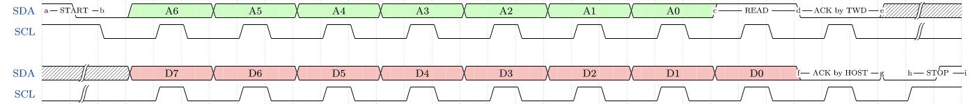
For a read operation the host first generates START or REPEATED-START condition. Then, the host transmits the 7 bit device
address (green signals A6 to A0) plus the read-command bit. If the transferred address matches the one programmed to to
TWD_CTRL_DEV_ADDR control register bits the TWD module will response with an ACK by pulling the SDA bus line actively
low during the 9th SCL clock pulse. If there is no address match the TWD will not interfere with the bus and will wait for
the next START or REPEATED-START condition.
For the actual data transmission the host keeps the SDA line at high state while sending the clock pulses. The TWD will read a byte from the internal TX FIFO and will transmit it MSB-first to the host. During the 9th clock pulse the host has to acknowledged the transfer (ACK) by pulling SDA low. If no ACK is received by the TWD no data is taken from the TX FIFO and the same byte is transmitted in the next data phase. If the TX FIFO becomes empty while the host keeps reading data, all-one bytes are sent back to the host. The transaction is terminated by a STOP condition.
Write Operation: Host Writes Data to TWD Module
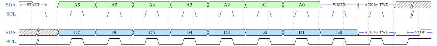
For a write operation the host first generates START or REPEATED-START condition. Then, the host transmits the 7 bit device
address (green signals A6 to A0) plus the write-command bit. If the transferred address matches the one programmed to to
TWD_CTRL_DEV_ADDR control register bits the TWD module will response with an ACK by pulling the SDA bus line actively
low during the 9th SCL clock pulse. If there is no address match the TWD will not interfere with the bus and will wait for
the next START or REPEATED-START condition.
For the actual data transmission the host sends the write-data MSB first together with the clock pulses. During the 9th clock pulse the TWD will respond with an ACK by pulling SDA low. Note that the TWD will respond with a NACK if the RX FIFO is full. The transaction is terminated by a STOP condition.
Communication Status
Actual communication with the TWD is (re-)started when a START or REPEATED-START condition followed by the TWD device
address is received. This communication is terminated as soon as a STOP condition is received. The current state of the
communication can be polled via the TWD_CTRL_COM control register flag.
Whenever a communication start has been observed the TWD_CTRL_COM_BEG control register flag becomes set.
Accordingly, the TWD_CTRL_COM_END control register flag becomes set whenever a communication end / termination
has been observed. These flags retain their value until they are either manually deleted (by writing a 1 to
the respective flag) or the TWD module is deactivated and thus reset.
TWD Interrupt
The TWD module provides a single interrupt to signal certain FIFO conditions and/or communication states to the CPU.
The control register’s TWD_CTRL_IRQ_* bits are used to enabled individual interrupt conditions. Note that all enabled
conditions are logically OR-ed.
| Interrupt Enable | Description | Interrupt Condition |
|---|---|---|
|
Interrupt if at least one data byte is available in the RX FIFO. |
|
|
Interrupt if the RX FIFO is full. |
|
|
Interrupt if the TX FIFO is empty. |
|
|
Interrupt if the TX FIFO is not full yet. |
|
|
Interrupt if a communication-start has been observed. |
|
|
Interrupt if a communication-end has been observed. |
|
The CPU interrupt request remains active until all enabled interrupt-causing conditions are resolved.
The interrupt can only trigger if the module is actually enabled (TWD_CTRL_EN is set).
Tristate Driver
The TWD module requires a single tristate drives (actually: open-drain drivers - signals can only be actively driven low) for the SDA line, which have to be implemented by the user in the setup’s top module / IO ring. The SCL signal is only read by the TWD module (input only) and therefore does not require a tristate driver. A generic VHDL example is shown below.
-- IO ports / bus lines --
sda_io : inout std_logic; -- bidirectional
scl_io : in    std_logic; -- input only

-- tristate driver --
sda_io <= '0' when (twd_sda_o = '0') else 'Z'; -- drive (pull low)

-- sense --
twd_sda_i <= std_ulogic(sda_io);
twd_scl_i <= std_ulogic(scl_io);
Register Map
| Address | Name [C] | Bit(s), Name [C] | R/W | Function |
|---|---|---|---|---|
|
|
|
r/w |
TWD enable, reset if cleared |
|
-/w |
Clear RX FIFO, flag auto-clears |
||
|
-/w |
Clear TX FIFO, flag auto-clears |
||
|
r/w |
Bus sample clock / filter select |
||
|
r/w |
Device address (7-bit) |
||
|
r/w |
IRQ if RX FIFO data available |
||
|
r/w |
IRQ if RX FIFO full |
||
|
r/w |
IRQ if TX FIFO empty |
||
|
r/w |
IRQ if TX FIFO is not full |
||
|
r/w |
IRQ if begin of communication |
||
|
r/w |
IRQ if end of communication |
||
|
r/- |
FIFO depth; log2( |
||
|
r/- |
FIFO depth; log2( |
||
|
r/- |
RX FIFO data available |
||
|
r/- |
RX FIFO full |
||
|
r/- |
TX FIFO empty |
||
|
r/- |
TX FIFO full |
||
|
r/c |
Communication has started; clear by writing 1 |
||
|
r/c |
Communication has ended; clear by writing 1 |
||
|
r/- |
Active communication |
||
|
|
|
r/w |
RX/TX data FIFO access |
|
r/- |
reserved, read as zero |
2.8.18. One-Wire Serial Interface Controller (ONEWIRE)
Hardware source files: |
neorv32_onewire.vhd |
|
Software driver files: |
neorv32_onewire.c |
|
neorv32_onewire.h |
||
Top entity ports: |
|
1-bit 1-wire bus sense input |
|
1-bit 1-wire bus output (pull low only) |
|
Configuration generics: |
|
implement ONEWIRE interface controller when |
|
RTX FIFO depth, has to be zero or a power of two, min 1 |
|
CPU interrupts: |
fast IRQ channel 13 |
operation done interrupt (see Processor Interrupts) |
Key Features
-
Dallas® 1-Wire™-compatible host controller
-
Hardware-based protocol handling (RESET, presence, data, etc.)
-
Fine-grained programmable bus timings
-
Optional data/command FIFO
-
Interrupt based on FIFO status
Overview
The NEORV32 ONEWIRE module implements a single-wire interface controller that is compatible to the Dallas/Maxim 1-Wire protocol, which is an asynchronous half-duplex bus requiring only a single signal wire (plus ground) for communication.
The bus is based on a single open-drain signal. The controller as well as all devices on the bus can only pull-down the bus (similar to TWI/I2C). The default high-level is provided by a single pull-up resistor connected to the positive power supply close to the bus controller. Recommended values are between 1kΩ and 10kΩ depending on the bus characteristics (wire length, number of devices, etc.).
Tri-State Drivers
The ONEWIRE module requires a tristate driver (actually, just an open-drain driver) for the 1-wire bus line, which has
to be implemented in the top module / IO ring of the design. A generic VHDL example is given below (onewire_io is the
actual 1-wire bus signal, which is of type std_logic; onewire_o and onewire_i are the processor’s ONEWIRE port signals).
onewire_io <= '0' when (onewire_o = '0') else 'Z'; -- drive (low)
onewire_i  <= std_ulogic(onewire_io); -- sense
Theory of Operation
The ONEWIRE controller provides two interface registers: CTRL and DCMD. The control register (CTRL)
is used to configure the module and to monitor the current state. The DCMD register, which can optionally
by buffered by a configurable FIFO (IO_ONEWIRE_FIFO generic), is used to read/write data from/to the bus
and to trigger bus operations.
The module is enabled by setting the ONEWIRE_CTRL_EN bit in the control register. If this bit is cleared, the
module is automatically reset, any bus operation is aborted, the bus is brought to high-level (due to the external
pull-up resistor) and the internal FIFO is cleared. The basic timing configuration is programmed via a coarse clock
prescaler (ONEWIRE_CTRL_PRSCx bits) and a fine clock divider (ONEWIRE_CTRL_CLKDIVx bits).
The controller can execute four basic bus operations, which are triggered by writing the according command bits
in the DCMD register (ONEWIRE_DCMD_DATA_* bits) while also writing the actual data bits (ONEWIRE_DCMD_CMD_*
bits).
-
0b00(ONEWIRE_CMD_NOP) - no operation (dummy) -
0b01(ONEWIRE_CMD_BIT) - transfer a single-bit (read-while-write) -
0b10(ONEWIRE_CMD_BYTE) - transfer a full-byte (read-while-write) -
0b11(ONEWIRE_CMD_RESET) - generate reset pulse and check for device presence
Every command (except NOP) will result in a bus operation when dispatched from the data/command FIFO.
Each command (except NOP) will also sample a bus response (a read bit, a read byte or a presence pulse) to a
shadowed receive FIFO that is accessed when reading the DCMD register.
When the single-bit operation (ONEWIRE_CMD_BIT) is executed, the data previously written to DCMD[0] will
be send to the bus and the response is sample to DCMD[7]. Accordingly, a full-byte transmission (ONEWIRE_CMD_BYTE)
will send the byte written to DCMD[7:0] to the bus and will sample the response to DCMD[7:0] (LSB-first). Finally, the
reset command (ONEWIRE_CMD_RESET) will generate a bus reset and will also sample the "presence pulse" from the device(s)
to the DCMD[ONEWIRE_DCMD_PRESENCE].
|
Read from Bus
In order to read a single bit from the bus DCMD[0] has to set to 1 before triggering the bit transmission
operation to allow the accessed device to pull-down the bus. Accordingly, DCMD[7:0] has to be set to 0xFF before
triggering the byte transmission operation when the controller shall read a byte from the bus.
|
As soon as the current bus operation has completed (and there are no further operations pending in the FIFO) the
ONEWIRE_CTRL_BUSY bit in the control registers clears.
Bus Timing
The control register provides a 2-bit clock prescaler select (ONEWIRE_CTRL_PRSC) and a 8-bit clock divider
(ONEWIRE_CTRL_CLKDIV) for timing configuration. Both are used to define the elementary base time Tbase.
All bus operations are timed using multiples of this elementary base time.
ONEWIRE_CTRL_PRSC[2:0] |
0b00 |
0b01 |
0b10 |
0b11 |
|---|---|---|---|---|
Resulting |
2 |
4 |
8 |
64 |
Together with the clock divider value (ONEWIRE_CTRL_PRSCx bits = clock_divider) the base time is defined by the
following formula:
Example:
-
fmain = 100MHz
-
clock prescaler select =
0b01→clock_prescaler= 4 -
clock divider
clock_divider= 249
The base time is used to coordinate all bus interactions. Hence, all delays, time slots and points in time are quantized as multiples of the base time Tbase. The following images show the two basic operations of the ONEWIRE controller: single-bit (0 or 1) transaction and reset with presence detect. Note that the full-byte operations just repeats the single-bit operation eight times. The relevant points in time are shown as absolute time points (in multiples of the time base Tbase) with the falling edge of the bus as reference points.
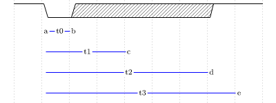
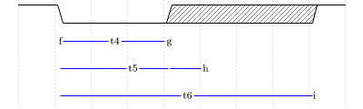
| Symbol | Description | Multiples of Tbase | Time when Tbase = 10µs |
|---|---|---|---|
Single-bit data transmission |
|||
|
Time until end of active low-phase when writing a |
1 |
10µs |
|
Time until controller samples bus state (read operation) |
2 |
20µs |
|
Time until end of bit time slot (when writing a |
7 |
70µs |
|
Time until end of inter-slot pause (= total duration of one bit) |
9 |
90µs |
Reset pulse and presence detect |
|||
|
Time until end of active reset pulse |
48 |
480µs |
|
Time until controller samples bus presence |
55 |
550µs |
|
Time until end of presence phase |
96 |
960µs |
|
Default Timing Parameters
The "known-good" default values for base time multiples were chosen for stable and reliable bus
operation and not for maximum throughput.
|
The absolute points in time are hardwired by the VHDL code and cannot be changed during runtime. However, the timing parameter can be customized (if necessary) by editing the ONEWIRE’s VHDL source file. The times t0 to t6 correspond to the previous timing diagrams.
neorv32_onewire.vhd-- timing configuration (absolute time in multiples of the base tick time t_base) --
constant t_write_one_c : unsigned(6 downto 0) := to_unsigned( 1, 7); -- t0
constant t_read_sample_c : unsigned(6 downto 0) := to_unsigned( 2, 7); -- t1
constant t_slot_end_c : unsigned(6 downto 0) := to_unsigned( 7, 7); -- t2
constant t_pause_end_c : unsigned(6 downto 0) := to_unsigned( 9, 7); -- t3
constant t_reset_end_c : unsigned(6 downto 0) := to_unsigned(48, 7); -- t4
constant t_presence_sample_c : unsigned(6 downto 0) := to_unsigned(55, 7); -- t5
constant t_presence_end_c : unsigned(6 downto 0) := to_unsigned(96, 7); -- t6|
Overdrive Mode
The ONEWIRE controller does not support the overdrive mode natively. However, it can be implemented by reducing
the base time Tbase (and by eventually changing the hardwired timing configuration in the VHDL source file).
|
Interrupt
A single interrupt is provided by the ONEWIRE module to signal "idle" condition to the CPU. Whenever the controller is idle (again) and the data/command FIFO is empty, the interrupt becomes active.
Register Map
| Address | Name [C] | Bit(s), Name [C] | R/W | Function |
|---|---|---|---|---|
|
|
|
r/w |
ONEWIRE enable, reset if cleared |
|
-/w |
clear RXT FIFO, auto-clears |
||
|
r/w |
2-bit clock prescaler select |
||
|
r/w |
8-bit clock divider value |
||
|
r/- |
reserved, read as zero |
||
|
r/- |
FIFO depth; log2( |
||
|
r/- |
reserved, read as zero |
||
|
r/- |
TX FIFO full |
||
|
r/- |
RX FIFO data available |
||
|
r/- |
current state of the bus line |
||
|
r/- |
operation in progress when set or TX FIFO not empty |
||
|
|
|
r/w |
receive/transmit data |
|
-/w |
operation command LSBs |
||
|
r/- |
bus presence detected |
||
|
r/- |
reserved, read as zero |
2.8.19. Pulse-Width Modulation Controller (PWM)
Hardware source files: |
neorv32_pwm.vhd |
|
Software driver files: |
neorv32_pwm.c |
|
neorv32_pwm.h |
||
Top entity ports: |
|
PWM output channels (32-bit) |
Configuration generics: |
|
number of PWM channels to implement (0..32) |
CPU interrupts: |
none |
Key Features
-
Up to 32 individual channels with up to 16-bit resolution and programmable polarity
-
Fast-PWM or phase-correct operation mode with counter-compare and counter-wrap registers
-
Toggle-free 0% and 100% duty cycle output rates
-
Global clock prescaler
Overview
The PWM module implements a pulse-width modulation controller with up to 32 independent channels. Period length (and thus, the carrier frequency), duty cycle, polarity and operation mode can be programmed individually for each channel. However, the clock for the PWM counter increment is defined by a single global clock prescaler. PWM operation is based on 16-bit wide period counters that are constrained by programmable wrapping values.
The total number of implemented channels is defined by the IO_PWM_NUM generic. The PWM output signal pwm_o has
a static size of 32 bit. Channel 0 corresponds to bit 0, channel 1 to bit 1 and so on. If less than 32 channels
are configured, only the LSB-aligned channel bits are connected while the remaining ones are hardwired to zero.
Theory of Operation
The PWM module provides several configuration registers: an ENABLE register, a POLARITY registers, a CLKPRSC
register, and a MODE register. Each of these register provides one bit (LSB-aligned) for each available PWM channel.
Additional, up to IO_PWM_NUM channel register CHANNEL are provided.
The ENABLE register is used to enable individual PWM channels. By using bit-masks several channels can be enabled
at once so they operate in perfect lockstep. The PWM counter of a disabled channel is halted and reset to zero; the
according PWM output (pwm_o(i)) is reset to the configured polarity. The polarity of each channel’s output can be
inverted by setting the corresponding bit in the POLARITY register.
The CLKPRSC register configures the global clock prescaler that is used for the PWM counter increment of all
channels. Eight pre-defined prescaler values are available:
CLKPRSC |
0b000 |
0b001 |
0b010 |
0b011 |
0b100 |
0b101 |
0b110 |
0b111 |
|---|---|---|---|---|---|---|---|---|
Resulting |
2 |
4 |
8 |
64 |
128 |
1024 |
2048 |
4096 |
The MODE register defines the PWM operation mode of a channel. If bit i is 0 channel i operates in
fast-PWM mode. If bit i is 1 channel i operates in phase-correct PWM mode.
Duty cycle and period length of each channel are defined by the according CHANNEL registers. These registers are
split in two half-words: the lowest half-word defines the counter-compare value (CMP) while the upper half-word defines
the counter-wrap value (TOP). Regardless of the configured PWM operation mode, the duty cycle of channel i is
defined by the following formula:
The NEORV32 PWM module supports toggle-free 0% and 100% duty cycle output rates. 0% duty cycle is achieved by
setting CMP = 0. 100% duty cycle is achieved by setting CMP = TOP + 1.
CHANNEL Half-Word AccessCHANNEL[i] registers can also be accessed using half-word
load/store operation. This allows to update TOP and CMP independent of each other.
|
Fast-PWM Mode
When in fast-PWM mode (MODE[i] = 0) the channel’s PWM counter generates a sawtooth-like waveform. The counter
automatically wraps to all-zero when reaching the programmed TOP[i] value. Whenever the counter value is less
equal to or greater than the CMP[i] value the PWM output is set to the programmed polarity (POLARITY[i])
value; otherwise it is set to the inverse polarity.
MODE[i] = 0

TOP[i] ---------------------/|--------------/|--------------/|--------------/
                          /  |            /  |            /  |            /
                        /    |          /    |          /    |          /
CMP[i] ---------------/------|--------/------|--------/------|--------/
                    / .      |      / .      |      / .      |      / .
                  /   .      |    /   .      |    /   .      |    /   .
                /     .      |  /     .      |  /     .      |  /     .
counter[i] ___/       .      |/       .      |/       .      |/       .
                      .      .        .      .        .      .        .
                      .      .        .      .        .      .        .
         -------------+      +--------+      +--------+      +--------+
pwm_o[i]              |      |        |      |        |      |        |       (POLARITY[i] = 0)
                      +------+        +------+        +------+        +------
                      .      .        .      .        .      .        .
                      .      .        .      .        .      .        .
                      +------+        +------+        +------+        +------
pwm_o[i]              |      |        |      |        |      |        |       (POLARITY[i] = 1)
         -------------+      +--------+      +--------+      +--------+
Based on the global clock prescaler and the TOP wrap value, the carrier frequency of a channel is defined by
the following formula (fmain is the main clock frequency of the processor; clock_prescaler is the global
pre-scaling factor according to the selected CLKPRSC value):
Phase-Correct PWM Mode
When in phase-correct PWM mode (MODE[i] = 1) the channel’s PWM counter generates a triangle-like waveform.
Phase-correct mode centers the pulse on the same point regardless of the duty cycle. After enabling, the PWM
counters counts upward until it reaches the TOP value. After that the counter counts downward
until it reaches 0 again. Whenever the counter value is equal to or greater than the CMP[i] value the PWM
output is set to the programmed polarity (POLARITY[i]) value; otherwise it is set to the inverse polarity.
MODE[i] = 1

TOP[i] ---------------------/\----------------------------/\
                          /    \                        /    \
                        /        \                    /        \
CMP[i] ---------------/------------\----------------/------------\
                    / .            . \            / .            . \
                  /   .            .   \        /   .            .   \
                /     .            .     \    /     .            .     \
counter[i] ___/       .            .       \/       .            .       \___
                      .            .                .            .
                      .            .                .            .
         -------------+            +----------------+            +-----------
pwm_o[i]              |            |                |            |            (POLARITY[i] = 0)
                      +------------+                +------------+
                      .            .                .            .
                      .            .                .            .
                      +------------+                +------------+
pwm_o[i]              |            |                |            |            (POLARITY[i] = 1)
         -------------+            +----------------+            +-----------
Based on the global clock prescaler and the TOP wrap value, the carrier frequency of a channel is defined
by the following formula (fmain is the main clock frequency of the processor; clock_prescaler is the
global pre-scaling factor according to the selected CLKPRSC value):
|
PWM Dead Time
The phase-correct PWM mode can also be used for controlling modules that require a certain dead time
(e.g. H-bridges). This requires two PWM channels, both of which operate in phase-correct mode, but the
second channel is configured with an inverse polarity. Both channels need to have the same TOP value
and must be enabled at once to have a perfect phase and frequency match. The dead time is define by
the difference of the channel’s CMP values:Tdead = 0.5 * T * ( CMP[i] - CMP[i+1])
|
Register Map
| Address | Name [C] | Bit(s) | R/W | Function |
|---|---|---|---|---|
|
|
|
r/w |
Channel enable, one bit per channel |
|
|
|
r/w |
Channel polarity, one bit per channel |
|
|
|
r/w |
Global clock prescaler select |
|
|
|
r/w |
Channel operation mode (0 = fast-PWM, 1 = phase-correct PWM), one bit per channel |
|
|
|
r/w |
Channel 0 full word access alias ( |
|
|
|
r/w |
Channel 0 top/wrap value register |
|
|
|
r/w |
Channel 0 compare value register |
… |
… |
… |
r/w |
… |
|
|
|
r/w |
Channel 31 full word access alias ( |
|
|
|
r/w |
Channel 31 top/wrap value register |
|
|
|
r/w |
Channel 31 compare value register |
2.8.20. True Random-Number Generator (TRNG)
Hardware source files: |
neorv32_trng.vhd |
|
Software driver files: |
neorv32_trng.c |
|
neorv32_trng.h |
||
Top entity ports: |
none |
|
Configuration generics: |
|
implement TRNG when |
|
data FIFO depth, min 1, has to be a power of two |
|
|
total number of ring-oscillators |
|
|
number of inverters in first ring-oscillator, has to be odd |
|
|
number of raw bits to process for one output byte, has to be power of two |
|
CPU interrupts: |
fast IRQ channel 15 |
data available interrupt (see Processor Interrupts) |
Key Features
-
True random number generator based on phase noise
-
Completely technology-independent architecture
-
Configurable TRNG layout to adjust to technology and quality requirements
-
Optional random data FIFO
-
Interrupt based on FIFO status
Overview
The NEORV32 true random number generator provides physically true random numbers. It is based on free-running ring-oscillators that generate phase noise when being sampled by a constant clock. This phase noise is used as physical entropy source. The TRNG features a platform independent architecture without FPGA-specific primitives, macros or attributes so it can be synthesized for any FPGA.
|
In-Depth Documentation
For more information about the neoTRNG architecture and an analysis of its random quality check out the
neoTRNG repository: https://github.com/stnolting/neoTRNG
|
|
Inferring Latches
The synthesis tool might emit warnings regarding inferred latches or combinatorial loops. However, this
is not design flaw as this is exactly what we want.
|
Theory of Operation
The TRNG provides two memory mapped interface register. One control register (CTRL) for configuration and
status check and one data register (DATA) for obtaining the random data. The TRNG is enabled by setting the
control register’s TRNG_CTRL_EN. As soon as the TRNG_CTRL_AVAIL bit is set a new random data byte is
available and can be obtained from the lowest 8 bits of the DATA register. If this bit is cleared, there
is no valid data available and the reading DATA will return all-zero.
The actual neoTRNG is configured by three generics:
-
IO_TRNG_NUM_ROdefines the total number of ring-oscillators. -
IO_TRNG_NUM_INVdefines the number of inverters in the first ring-oscillator. Each subsequent RO is two inverters longer than the previous one. -
IO_TRNG_NUM_RBITdefines the number of raw entropy bits obtained from the ring-oscillators that are scrmabled and combined to produce a single random output byte.
An internal entropy FIFO can be configured using the IO_TRNG_FIFO generic. This FIFO automatically samples
new random data from the TRNG to provide some kind of random data pool for applications which require a
larger number of random data in a short time. The random data FIFO can be cleared at any time either by
disabling the TRNG or by setting the TRNG_CTRL_FIFO_CLR flag. The FIFO depth can be retrieved by software
via the TRNG_CTRL_FIFO_* bits.
|
Simulation
When simulating the processor the TRNG is automatically set to "simulation mode". In this mode the physical
entropy sources (the ring-oscillators) are replaced by a simple pseudo RNG based on a LFSR providing only
deterministic pseudo-random data. The TRNG_CTRL_SIM_MODE flag of the control register is set if simulation
mode is active.
|
Interrupt
The TRNG provides a single interrupt request signal that gets triggered when the TRNG is enabled and the
data FIFO is completely full (indicating that at least IO_TRNG_FIFO bytes of random data are available).
Register Map
| Address | Name [C] | Bit(s), Name [C] | R/W | Function |
|---|---|---|---|---|
|
|
|
r/w |
TRNG enable |
|
-/w |
flush random data FIFO when set; auto-clears |
||
|
r/- |
simulation mode (PRNG!) |
||
|
r/- |
random data available when set |
||
|
r/- |
FIFO depth ( |
||
|
r/- |
FIFO depth ( |
||
|
r/- |
Total number of ring-oscillators ( |
||
|
r/- |
Number of inverters in first ring-oscillator ( |
||
|
|
|
r/- |
random data byte |
|
r/- |
reserved, read as zero |
2.8.21. Custom Functions Subsystem (CFS)
Hardware source files: |
neorv32_cfs.vhd |
|
Software driver files: |
neorv32_cfs.c |
|
neorv32_cfs.h |
||
Top entity ports: |
|
custom input conduit, 256-bit |
|
custom output conduit, 256-bit |
|
Configuration generics: |
|
implement CFS when |
CPU interrupts: |
fast IRQ channel 1 |
CFS interrupt (see Processor Interrupts) |
Key Features
-
Tightly-coupled co-processor unit for custom hardware accelerators
-
Can operate independently of the CPU
-
CPU access via memory-mapped registers (16kB)
-
Custom 256-bit input and output conduits for custom IO
Overview
The custom functions subsystem is meant for implementing custom tightly-coupled co-processors or interfaces.
It provides up to 16384 32-bit memory-mapped read/write registers (REG, see register map below) that can be
accessed by the CPU via normal load/store operations. The actual functionality of these register has to be
defined by the hardware designer. Furthermore, the CFS provides two input/output conduits to implement custom
on-chip or off-chip interfaces.
Just like any other externally-connected IP, logic implemented within the custom functions subsystem can operate independently of the CPU providing true parallel processing capabilities. Potential use cases might include dedicated hardware accelerators for en-/decryption (AES), signal processing (FFT) or AI applications (CNNs) as well as custom IO systems like fast memory interfaces (DDR) and mass storage (SDIO), networking (CAN) real-time data transport (I2S) or just replication of existent NEORV32 peripherals.
|
Custom ISA Instructions
If you like to implement custom instructions that are executed right within the CPU’s ALU
see the Xcfu ISA Extension and the according Custom Functions Unit (CFU).
|
|
CFS Template
Take a look at the template CFS VHDL source file (rtl/core/neorv32_cfs.vhd). The file is highly
commented to illustrate all aspects that are relevant for implementing custom CFS-based co-processor designs.
|
CFS Software Access
The CFS memory-mapped registers can be accessed by software using the provided C-language aliases (see
register map table below). Note that all interface registers are defined as 32-bit words of type uint32_t.
// C-code CFS usage example
NEORV32_CFS->REG[0] = (uint32_t)some_data_array(i); // write to CFS register 0
int temp = (int)NEORV32_CFS->REG[20]; // read from CFS register 20
CFS Custom IOs
The CFS provides two unidirectional input and output conduits cfs_in_i and cfs_out_o. Both signals
are 512 bit wide and are are directly propagated to the processor’s top entity. These conduits can be used
to implement application-specific interfaces like memory or peripheral connections. The actual use case of
these signals has to be defined by the hardware designer.
CFS Interrupt
The CFS provides a single high-level-triggered interrupt request signal mapped to the CPU’s fast interrupt channel 1.
Register Map
| Address | Name [C] | Bit(s) | R/W | Function |
|---|---|---|---|---|
|
|
|
(r)/(w) |
custom CFS register 0 |
|
|
|
(r)/(w) |
custom CFS register 1 |
… |
… |
|
(r)/(w) |
… |
|
|
|
(r)/(w) |
custom CFS register 16382 |
|
|
|
(r)/(w) |
custom CFS register 16383 |
2.8.22. Smart LED Interface (NEOLED)
Hardware source files: |
neorv32_neoled.vhd |
|
Software driver files: |
neorv32_neoled.c |
|
neorv32_neoled.h |
||
Top entity ports: |
|
1-bit serial data output |
Configuration generics: |
|
implement NEOLED controller when |
|
transmission FIFO depth, has to be a power of 2, min 1 |
|
CPU interrupts: |
fast IRQ channel 9 |
configurable NEOLED data FIFO interrupt (see Processor Interrupts) |
Key Features
-
"NeoPixel™"-compatible LED controller
-
Hardware-based protocol handling
-
Fine-grained programmable bus timings
-
Optional data/command FIFO
-
Interrupt based on FIFO status
Overview
The NEOLED module provides a dedicated interface for "smart LEDs" like WS2812, WS2811 and other compatible ones. These LEDs provide a single-wire interface that uses an asynchronous serial protocol for transmitting data. The NEOLED module handles the tight timing constraints of the interface entirely in hardware. A configurable data and command buffer (FIFO) allows to utilize (e.g. DMA-backed) block transfer operation without CPU intervention.
LEDs are connected to the neoled_o output and can be arbitrarily chained. The module also supports 24-bit and
32-bit LED data Hence, mixed setups with RGB LEDs (24-bit color) and RGBW LEDs (32-bit color including a dedicated
white LED chip) are fully supported.
The NEOLED modules provides four accessible interface registers: the control register CTRL and the write-only
DATA24, DATA32 and STROBE registers. The precise interface timing is configured via the control registers.
The data and strobe registers are used for sending 24-bit/32-bit data and reset/strobe commands.
Protocol
The interface of the smart LEDs is based on duty-cycle modulation of a specific carrier signal. Data is transmitted in a serial manner starting with the MSB. The intensity for each R/G/B (/W) LED chip is defined via an 8-bit value. The actual data bits are transferred by modifying the duty cycle of the base carriers. A RESET command is send by pulling the data line LOW for at least 50μs.
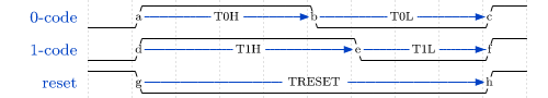
Ttotal (Tcarrier) |
1.25μs +/- 300ns |
period for a single bit |
T0H |
0.4μs +/- 150ns |
high-time for sending a |
T0L |
0.8μs +/- 150ns |
low-time for sending a |
T1H |
0.85μs +/- 150ns |
high-time for sending a |
T1L |
0.45μs +/- 150 ns |
low-time for sending a |
RESET |
Above 50μs |
low-time for sending a RESET command |
Timing Configuration
The basic carrier frequency (800kHz for the WS2812 LEDs) is configured via a 3-bit clock prescaler
(NEOLED_CTRL_PRSC*, see table below) that scales the main processor clock fmain and a 5-bit cycle
multiplier NEOLED_CTRL_T_TOT_*.
NEOLED_CTRL_PRSC[2:0] |
0b000 |
0b001 |
0b010 |
0b011 |
0b100 |
0b101 |
0b110 |
0b111 |
|---|---|---|---|---|---|---|---|---|
Resulting |
2 |
4 |
8 |
64 |
128 |
1024 |
2048 |
4096 |
The duty-cycles (or more precisely: the high- and low-times for sending either a '1' bit or a '0' bit) are
defined via the 5-bit NEOLED_CTRL_T_1H_* and NEOLED_CTRL_T_0H_* values, respectively. These programmable
timing constants allow to adapt the interface for a wide variety of smart LED protocols.
Timing Configuration - Example (WS2812)
Generate the base clock fTX for the NEOLED TX engine:
-
processor clock fmain = 100 MHz
-
NEOLED_CTRL_PRSCx=0b001= fmain / 4
Generate carrier period (Tcarrier) and high-times (duty cycle) for sending 0 (T0H) and 1 (T1H) bits:
-
NEOLED_CTRL_T_TOT=0b11110(= decimal 30) -
NEOLED_CTRL_T_0H=0b01010(= decimal 10) -
NEOLED_CTRL_T_1H=0b10100(= decimal 20)
The NEOLED SW driver library (neorv32_neoled.h) provides a simplified configuration
function that configures all timing parameters for driving WS2812 LEDs based on the processor
clock frequency.
|
NEOLED Data/Command (FIFO)
The interface features a configurable TX data and command buffer (a FIFO) to allow more CPU-independent operation.
The buffer depth is configured via the IO_NEOLED_TX_FIFO top generic. The FIFO size configuration can be
read by software from the NEOLED_CTRL_FIFO_x control register bits. If the module is disabled by clearing
NEOLED_CTRL_EN the entire data and command buffer is cleared.
LED data and commands are written to the DATA24, DATA32 and STROBE registers, which are transparently buffered
by the optional FIFO. Writing data to DATA24 will finally transmit the 24 LSB-aligned bits from the written data
word to the LED string. Writing data to DATA32 will finally transmit all 32-bit bits from the written data word to
the LED string. Writing any data to STROBE, which is also buffered by the FIFO, will send a STROBE (RESET) command
to the LED string.
Software can check the FIFO fill level via the control register’s NEOLED_CTRL_TX_EMPTY and NEOLED_CTRL_TX_FULL
flags. The NEOLED_CTRL_TX_BUSY flag provides additional information if the serial transmit engine is still busy
sending data.
NEOLED Interrupt
The NEOLED modules features a single interrupt that gets triggered when the TX data/command FIFO is empty.
Register Map
| Address | Name [C] | Bit(s), Name [C] | R/W | Function |
|---|---|---|---|---|
|
|
|
r/w |
module enable |
|
r/w |
clock prescaler select |
||
|
r/w |
pre-scaled clock ticks per total single-bit period (Ttotal) |
||
|
r/w |
pre-scaled clock ticks per high-time for sending a zero-bit (T0H) |
||
|
r/w |
pre-scaled clock ticks per high-time for sending a one-bit (T1H) |
||
|
r/- |
reserved, read as zero |
||
|
r/w |
log(FIFO size) |
||
|
r/- |
TX FIFO is empty |
||
|
r/- |
TX FIFO is full |
||
|
r/- |
TX serial engine is busy when set |
||
|
|
|
-/w |
write 24-bit RGB data to transmission buffer |
|
|
|
-/w |
write 32-bit RGB data to transmission buffer |
|
|
- |
-/w |
write strobe/reset command to transmission buffer |
2.8.23. General Purpose Timer (GPTMR)
Hardware source files: |
neorv32_gptmr.vhd |
|
Software driver files: |
neorv32_gptmr.c |
|
neorv32_gptmr.h |
||
Top entity ports: |
none |
|
Configuration generics: |
|
number of individual GPTMR timer slices (0..16) |
CPU interrupts: |
fast IRQ channel 12 |
timer interrupt (see Processor Interrupts) |
Key Features
-
Up to 16 individual timer slices with 32-bit-wide timer and timer-match registers
-
Per-slice enable, mode and interrupt control/status
-
Single-shot or interval operation mode
-
Global clock prescaler
Overview
The general purpose timer module provides up to 16 individual timers organized as slices (the number of
implemented slices is configured by IO_GPTMR_NUM. Each slice can operate as single-shot timer or as
continuous/interval timer and provides a 32-bit counter (SLICE[i].CNT) and a 32-bit threshold registers
(SLICE[i].THR). Operation is controlled by two 32-bit control and status registers (CSR0 and CSR1).
An interrupt is triggered when a slice counter matches the according threshold value.
|
CSR Access
CSR0 and CSR1 can be accessed in full-word mode (CSR[0/1].WORD) and also in half-word
mode (e.g. CSR0.ENABLE) to update configuration sub-words with a single memory operation.
|
Theory of Operation
A slice i is enabled when the according bit of CSR0.ENABLE is set. Only the lowest IO_GPTMR_NUM
bits are available. When enabled, the slice`s counter register SLICE[i].CNT starts incrementing at
a prescaled clock frequency. This prescaler is globally configured (= for all slices) by the
CSR1.PRSC register:
CSR1.PRSC |
0b000 |
0b001 |
0b010 |
0b011 |
0b100 |
0b101 |
0b110 |
0b111 |
|---|---|---|---|---|---|---|---|---|
Resulting |
2 |
4 |
8 |
64 |
128 |
1024 |
2048 |
4096 |
When SLICE[i].CNT matches the threshold value in SLICE[i].THR the according interrupt-pending bit in
CSR1.IRQ becomes set. Disabled slices (CSR0.ENABLE(i) = 0) cannot generate any new interrupt requests.
However, pending interrupt in CSR1.IRQ will remain pending even if the according slice is disabled via.
Software can clear pending interrupts by writing zero to the according CSR1.IRQ bits. A CPU interrupt
request is generates if any slice interrupt i is pending and slice i is enabled (CSR0.ENABLE(i) = 1
and CSR1.IRQ(i) = 1).
The time until a slice interrupt is triggered (T[i]) depends on the processor clock (fmain) global
clock prescaler (selected by CSR1.PRSC) and the slice threshold value (SLICE[i].THR):
Each slice can operate as single-shot timer or as continuous interval timer: If CSR0.MODE(i) = 0
the according slice operates in single-shot mode: if the counter matches the programmed threshold
(SLICE[i].CNT == SLICE[i].THR) the slice interrupt becomes pending and the counter stops at the
threshold value. If CSR0.MODE(i) = 1 the according slice operates in continuous mode: if the
counter matches the programmed threshold (SLICE[i].CNT == SLICE[i].THR) the slice interrupt becomes
pending and the counter is reset to zero and starts counting again up to the threshold value.
Register Map
| Address | Name [C] | Bit(s), Name [C] | R/W | Description |
|---|---|---|---|---|
|
|
|
r/w |
Control and status register 0 full-word access. |
|
|
|
r/w |
Control and status register 0 - Slice enable (one bit per implemented slice starting at LSB). |
|
|
|
r/w |
Control and status register 0 - Slice operation mode: 0 = single shot, 1 = continuous (one bit per implemented slice starting at LSB). |
|
|
|
r/w |
Control and status register 1 full-word access. |
|
|
|
r/w |
Control and status register 1 - Slice interrupt pending (one bit per implemented slice starting at LSB); write 0 to clear interrupt. |
|
|
|
r/w |
Control and status register 1 - Global clock prescaler select. |
|
|
|
r/w |
Slice 0 counter register. |
|
|
|
r/w |
Slice 0 threshold register. |
… |
… |
… |
… |
… |
|
|
|
r/w |
Slice 15 counter register. |
|
|
|
r/w |
Slice 15 threshold register. |
2.8.24. Execution Trace Buffer (TRACER)
Hardware source files: |
neorv32_tracer.vhd |
|
Software driver files: |
neorv32_tracer.c |
|
neorv32_tracer.h |
||
Top entity ports: |
none |
|
Configuration generics: |
|
implement TRACER module when |
|
trace buffer depth, has to be zero or a power of two, min 1 |
|
|
write full trace log to file when |
|
CPU interrupts: |
fast IRQ channel 5 |
tracing stop-address match interrupt (see Processor Interrupts) |
Key Features
-
Delta-tracing of instruction execution
-
Auto-stop tracing (and issue interrupt) when reaching a programmable instruction address
-
Dump and inspect delta-trace directly from the firmware or via GDB
Overview
The NEORV32 tracer module allows to record program execution in order to find out how the CPU arrived at a certain code point. It is fed by the CPU’s Execution Trace Port. In order to keep the data rate low, so-called instruction delta tracing is used:
Instruction delta tracing, also known as branch tracing, works by tracking execution from a known start address by sending information about the deltas taken by the program. Deltas are typically introduced by jump, call, return and branch type instructions, although interrupts and exceptions are also types of deltas. Instruction delta tracing provides an efficient encoding of an instruction sequence by exploiting the deterministic way the processor behaves based on the program it is executing.
github.com/riscv-non-isa/riscv-trace-spec
This means that only non-linear changes of the program counter are recorded. These deltas are stored in a
a local memory (the trace buffer) and can be read by the debugger (e.g. GDB). The size of this trace buffer
is configurable via the IO_TRACER_BUFFER generic.
The program being executed can also read the trace buffer itself (stand-alone-mode, not debugger required). In the dual-core configuration, for example, one CPU core can analyze the trace of the other CPU core.
|
TRACER Demo Program
A demo program for the tracer can be found in sw/example/demo_tracer.
|
Theory of Operation
The tracer module provides four memory-mapped registers: the status and control register CTRL, a "stop-tracing"
address register STOP_ADDR and two read-only registers to read trace data (DELTA_SRC and DELTA_DST).
The trace module is enabled by setting the TRACER_CTRL_EN bit in the control register. If this bit is cleared,
the module i enabled and the internal trace buffer is cleared. Bit TRACER_CTRL_HSEL selects the hart / CPU core
that shall be traced. This bit is read-only zero for the single-core configuration.
Tracing is started by writing 1 to the TRACER_CTRL_START control register bit. Tracing can be stopped at any
time by manually writing 1 to the TRACER_CTRL_START control register bit. Software can check if tracing is
in progress by reading the TRACER_CTRL_RUN. Tracing is automatically stopped when program execution reaches
the address in the STOP_ADDR register. Automatic trace stopping can be disabled by writing -1 to this register.
|
Halt Tracing during Debug-Mode
Whenever the CPU enters debug mode, either by a halt request from the debugger or by a (hard-coded) breakpoint or
watchpoint, tracing is paused until the CPU resumes normal operation.
|
During tracing, the module writes the instruction deltas to the internal buffer. The buffer is implemented as FIFO,
so that only the last IO_TRACER_BUFFER instruction deltas are kept. At least one instruction delta is available
in the trace buffer when TRACER_CTRL_AVAIL is set. A single entry ("packet") of the trace buffer data can be read
via the two registers DELTA_SRC and DELTA_DST:
-
DELTA_SRCprovides the 31-bit instruction address of the branch source. Bit 0 is set if this trace packet is the very first after trace start; it is cleared for all further packets. -
DELTA_DSTprovides the 31-bit instruction address of the branch destination. Bit 0 is set if this branch was caused by a trap-entry; it is cleared if this branch was caused by a jump/call/branch instruction.
|
Trace Buffer Read Access
The trace buffer’s FIFO read-pointer automatically increments when reading DELTA_DST,
so make sure to read DELTA_SRC before DELTA_DST. The implementation as FIFO also
means that the trace data can only be read once.
|
Tracer Interrupt
The tracer module features a single interrupt that gets triggered when the traced program reached the address
stored in the module’s STOP_ADDR register. The pending interrupt needs to be explicitly acknowledged/cleared
by writing 1 to the TRACER_CTRL_IRQ_CLR control register bit.
Evaluating Trace Data from GDB
Two simple functions for handling the tracer are implemented as GDB script. The script is located in the tracer
example program and can be imported into GDB using the source command:
(gdb) source path/to/neorv32/sw/example/demo_tracer/neorv32_tracer.gdbAfter sourcing, two additional commands are available that can be executed from the GDB command line:
-
tracer_get: read-out the data from the trace buffer and print the execution history -
tracer_start arg: restart the tracer; the CPU ID has to be provided as argument (arg, 0 or 1)
Using the tracer from GDB is briefly illustrated in the following example:
neorv32/sw/example/demo_tracer)(gdb) make clean elf (1)
...
(gdb) load (2)
...
(gdb) c (3)
...
(gdb) source neorv32_tracer.gdb (4)
(gdb) tracer_get (5)
[0] SRC: 0x3b0 -> DST: 0x2cc <TRACE_START>
Line 128 of "main.c" starts at address 0x3b0 <main+212> and ends at 0x3b4 <main+216>.
Line 68 of "main.c" starts at address 0x2cc <test_code> and ends at 0x2d0 <test_code+4>.
...| 1 | Compile the demo program. |
| 2 | Upload the compiled ELF. |
| 3 | Start executing. The program will stop re-entering debug-mode when reaching main’s return statement. |
| 4 | Import the tracer helper functions script. |
| 5 | Get trace log and print. |
Tracer Simulation Logging
|
Simulation-Only
This feature is available in simulation only.
|
The NEORV32 tracer module can also be used to generate a complete log of all executed instructions. Simulation
trace logging is enabled by the IO_TRACER_SIMLOG_EN top generic. This also requires the tracer is implemented
(IO_TRACER_EN = true). However, no specific configuration of the control register CTRL is required. During
simulation, all traced instructions are written to log files in the simulator’s home folder:
-
neorv32.tracer0.logfor CPU 0 -
neorv32.tracer1.logfor CPU 1 (only if Dual-Core Configuration is enabled)
The trace log is structured line by line where each line describes an executed instruction. The start of an exemplary trace log might look like this:
neorv32.tracer1.log showing boot of core 1)52168 256630 0x000024f6 0xc00026f3 U csrrs x13, cycle, x0
52169 256633 0x000024fa 0xc02025f3 U csrrs x11, instret, x0
52170 256635 0x000024fe 0x0001 U c.addi x0, x0, 0
52171 256647 0x00002500 0x0001 U c.addi x0, x0, 0
52172 256650 0x00002502 0xc0002673 U csrrs x12, cycle, x0
52173 256653 0x00002506 0xc0202573 U csrrs x10, instret, x0
52174 256656 0x0000250a 0x00000073 U ecall
52175 256665 0x00003e94 0x34011073 M csrrw x0, mscratch, x2 <TRAP_ENTRY> (1)
52176 256667 0x00003e98 0x7119 M c.addi16sp x2, x2, -128
52177 256672 0x00003e9a 0xc206 M c.swsp x1, 4(x2)
52178 256675 0x00003e9c 0x340110f3 M csrrw x1, mscratch, x2| 1 | This line is used for explanation (see below). |
Column structure:
-
52175: Instruction index ("order"); a linear increasing counter that starts at zero and increments with each executed instruction; printed as decimal integer. -
256665: Time stamp; a linear increasing counter that starts at zero and increments with each clock cycle; printed as decimal integer. -
0x00003e94: Instruction address (program counter); printed as hexadecimal 32-bit value (0xprefix). -
0x34011073: instruction word; printed as 32-bit or 16-bit (compressed isntructgion) hexadecimal value (0xprefix). -
M: Current operating mode / privilege level (M= machine-mode,U= user-mode,D= debug-mode); printed as single character. -
csrrw: The decoded instruction mnemonic. For unknown instructionsINVALIDis printed instead. Decompressed 16-bit instructions have a prefixedc.(e.g.c.addi). -
x0, mscratch, x2: Operands of the decoded instruction. -
If the CPU encounters a trap (synchronous exception or interrupt)
<TRAP_ENTRY>is printed at the end of the line corresponding to the first instruction of the trap handler.
|
Instruction Execution Time
The execution time of instruction i (number of cycles required for retiring) can be calculated by
subtracting the current time stamp i from the next time stamp i+1.
|
Register Map
| Address | Name [C] | Bit(s), Name [C] | R/W | Function |
|---|---|---|---|---|
|
|
|
r/w |
TRACER enable, reset module when 0 |
|
r/w |
Hart select for tracing ( |
||
|
r/w |
Start tracing, flag always reads as zero |
||
|
r/w |
Manually stop tracing, flag always reads as zero |
||
|
r/- |
Tracing in progress when set |
||
|
r/- |
Trace data available when set |
||
|
r/w |
Clear pending interrupt when writing |
||
|
r/- |
|
||
|
r/- |
reserved, hardwired to zero |
||
|
|
|
r/w |
Stop-tracing-address register |
|
|
|
r/- |
Branch source address, set to |
|
r/- |
|
||
|
|
|
r/- |
Branch destination address |
|
r/- |
|
2.8.25. System Configuration Information Memory (SYSINFO)
Hardware source files: |
neorv32_sysinfo.vhd |
|
Software driver files: |
neorv32_sysinfo.h |
|
Top entity ports: |
none |
|
Configuration generics: |
all |
most of the top’s configuration generics |
CPU interrupts: |
none |
Key Features
-
Provides detailed SoC configuration information
Overview
The SYSINFO module allows the application software to determine the setting of most of the Processor Top Entity - Generics that are related to CPU and processor/SoC configuration. This device is always implemented - regardless of the actual hardware configuration since the NEORV32 software framework requires information from this device for correct operation. However, advanced users that do not want to use the default NEORV32 software framework can choose to disable the entire SYSINFO module. This might also be suitable for setups that use the processor just as wrapper for a CPU-only configuration.
Register Map
All registers of this module are read-only except for the CLK register. Upon reset, the CLK registers is initialized
from the CLOCK_FREQUENCY top entity generic. Application software can override this default value in order, for example,
to take into account a dynamic frequency scaling of the processor.
| Address | Name [C] | R/W | Description |
|---|---|---|---|
|
|
r/w |
clock frequency in Hz (initialized from top’s |
|
|
r/- |
miscellaneous system configurations (see SYSINFO - Miscellaneous Configuration) |
|
|
r/- |
specific SoC configuration (see SYSINFO - SoC Configuration) |
|
|
r/- |
cache configuration information (see SYSINFO - Cache Configuration) |
SYSINFO - Miscellaneous Configuration
| Byte | Name [C] | Description |
|---|---|---|
|
|
log2(internal IMEM size in bytes), via top’s |
|
|
log2(internal DMEM size in bytes), via top’s |
|
|
number of physical CPU cores ("harts") |
|
|
boot mode configuration, via top’s |
|
|
log2(internal bus timeout cycles), see Bus Monitor and Timeout |
|
|
log2(external bus timeout cycles), see Bus Monitor and Timeout |
SYSINFO - SoC Configuration
| Bit | Name [C] | Description |
|---|---|---|
|
|
set if processor-internal bootloader is implemented (via top’s |
|
|
set if external bus interface is implemented (via top’s |
|
|
set if processor-internal DMEM is implemented (via top’s |
|
|
set if processor-internal IMEM is implemented (via top’s |
|
|
set if on-chip debugger is implemented (via top’s |
|
|
set if processor-internal instruction cache is implemented (via top’s |
|
|
set if processor-internal data cache is implemented (via top’s |
|
- |
reserved, read as zero |
|
- |
reserved, read as zero |
|
- |
reserved, read as zero |
|
- |
reserved, read as zero |
|
|
set if on-chip debugger authentication is implemented (via top’s |
|
|
set if processor-internal IMEM is implemented as pre-initialized ROM (via top’s |
|
|
set if TWD is implemented (via top’s |
|
|
set if direct memory access controller is implemented (via top’s |
|
|
set if GPIO is implemented (via top’s |
|
|
set if CLINT is implemented (via top’s |
|
|
set if primary UART0 is implemented (via top’s |
|
|
set if SPI is implemented (via top’s |
|
|
set if TWI is implemented (via top’s |
|
|
set if PWM is implemented (via top’s |
|
|
set if WDT is implemented (via top’s |
|
|
set if custom functions subsystem is implemented (via top’s |
|
|
set if TRNG is implemented (via top’s |
|
|
set if SDI is implemented (via top’s |
|
|
set if secondary UART1 is implemented (via top’s |
|
|
set if smart LED interface is implemented (via top’s |
|
|
set if execution tracer is implemented (via top’s |
|
|
set if GPTMR is implemented (via top’s |
|
|
set if stream link interface is implemented (via top’s |
|
|
set if ONEWIRE interface is implemented (via top’s |
|
|
set if NEORV32 is being simulated |
SYSINFO - Cache Configuration
The SYSINFO cache register provides information about the configuration of the processor caches:
| Bit | Name [C] | Description |
|---|---|---|
|
|
log2(cache block size in bytes), via top’s |
|
|
log2(i-cache number of cache blocks), via top’s |
|
|
log2(d-cache number of cache blocks), via top’s |
|
|
start of non-cached address space, 256MB page, via top’s |
|
|
cache burst transfers enabled, via top’s |
|
- |
reserved, read as zero |
3. NEORV32 Central Processing Unit (CPU)
The NEORV32 CPU is an area-optimized RISC-V core implementing the rv32i_zicsr_zifencei base (privileged) ISA and
supporting several additional/optional ISA extensions. The CPU’s micro architecture is based on a von-Neumann
machine build upon a mixture of multi-cycle and pipelined execution schemes. Optionally, the core can be implemented
as SMP Dual-Core Configuration.
|
RISC-V Specifications
This chapter assumes that the reader is familiar with the official
RISC-V User and Privileged Architecture specifications.
|
Section Structure
3.1. CPU Top Entity - Signals
The following table shows all interface signals of the CPU top entity rtl/core/neorv32_cpu.vhd. All ports
(except for the data/instruction bus interfaces) use std_ulogic or std_ulogic_vector types, respectively.
The bus ports are wrapped as custom interface types (bus_req_t and bus_rsp_t). See section Bus Interface
for the protocol and type documentation.
| Signal | Width/Type | Dir | Description |
|---|---|---|---|
Clock and Reset |
|||
|
1 |
in |
Global clock line, all registers triggering on rising edge. |
|
1 |
in |
Global reset, low-active. |
Status |
|||
|
64 |
in |
System time from the Core-Local Interruptor (CLINT) (MTIME). |
|
|
out |
|
|
1 |
out |
Set while the CPU is in Sleep Mode. |
Interrupts (Traps, Exceptions and Interrupts) |
|||
|
1 |
in |
RISC-V machine software interrupt. |
|
1 |
in |
RISC-V machine external interrupt. |
|
1 |
in |
RISC-V machine timer interrupt. |
|
16 |
in |
Custom fast interrupt request signals. |
|
1 |
in |
Request CPU to halt and enter debug mode (RISC-V On-Chip Debugger (OCD)). |
Instruction Bus Interface |
|||
|
1 |
out |
Instruction fence / memory ordering. |
|
|
out |
Instruction fetch bus request. |
|
|
in |
Instruction fetch bus response. |
Data Bus Interface |
|||
|
1 |
out |
Data fence / memory ordering. |
|
|
out |
Data access (load/store) bus request. |
|
|
in |
Data access (load/store) bus response. |
3.2. CPU Top Entity - Generics
Most of the CPU configuration generics are a subset of the Processor Top Entity - Generics and are not listed here. However, the CPU provides some specific generics that are used to configure the CPU for the NEORV32 processor setup. These generics are assigned by the processor setup only and are not available for user defined configuration. The specific generics are listed below.
|
Table Abbreviations
The generic type "suv(x:y)" represents a std_ulogic_vector(x downto y).
|
| Name | Type | Description |
|---|---|---|
|
natural |
ID of the core (for |
|
suv(31:0) |
Vendor ID (for |
|
suv(31:0) |
CPU reset address. See section Address Space. |
|
suv(31:0) |
"Park loop" entry address for the On-Chip Debugger (OCD), has to be 4-byte aligned. |
|
suv(31:0) |
"Exception" entry address for the On-Chip Debugger (OCD), has to be 4-byte aligned. |
|
boolean |
Implement RISC-V-compatible "debug" CPU operation mode required for the On-Chip Debugger (OCD). |
|
boolean |
Implement RISC-V-compatible Trigger Module. See section On-Chip Debugger (OCD). |
|
boolean |
Implement RISC-V-compatible physical memory protection (PMP). See section |
|
natural |
Number of hardware triggers for the Trigger Module |
|
Tuning Option Generics
Additional generics that are related to certain tuning options are listed in section CPU Tuning Options.
|
3.3. Architecture
The CPU implements a pipelined multi-cycle architecture: each instruction is executed as a series of consecutive micro-operations. In order to increase performance, the CPU’s front-end (instruction fetch) and back-end (instruction execution) are de-couples via a FIFO (the instruction prefetch buffer. Thus, the front-end can already fetch new instructions while the back-end is still processing the previously-fetched instructions.
Basically, the CPU’s micro architecture is somewhere between a classical pipelined architecture, where each stage requires exactly one processing cycle (if not stalled) and a classical multi-cycle architecture, which executes every single instruction (including fetch) in a series of consecutive micro-operations. The combination of these two design paradigms allows an increased instruction execution in contrast to a pure multi-cycle approach (due to overlapping operation of fetch and execute) at a reduced hardware footprint (due to the multi-cycle concept).
As a Von-Neumann machine, the CPU provides independent interfaces for instruction fetch and data access. However, these two bus interfaces are merged into a single processor-internal bus via a prioritizing bus switch (data accesses have higher priority). Hence, all memory addresses including peripheral devices are mapped to a single unified 32-bit Address Space.
|
No Hardware Support for Misaligned Memory Accesses
The CPU does not support resolving unaligned memory access by the hardware. Any kind of
unaligned memory access will raise an exception to allow a software-based emulation.
See section Application Context Handling for more information.
|
3.3.1. CPU Front-End
The front-end is responsible for fetching instructions in chunks of 32-bits. This can be a single aligned 32-bit instruction, two 16-bit instructions or a mixture of both. Unaligned 32bit instructions are explicitly supported. The instruction chunks are queued within the instruction prefetch buffer (IPB). A consecutive logic reads data from this FIFO, optionally decompresses 16-bit instructions and assembles 32-bit instruction words that are forwarded to the CPU back-end for execution.
The IPB allows the front-end to do "speculative" instruction fetches as it keeps fetching the next consecutive instruction all the time. This also allows to decouple instruction fetch and instruction execution so both stages can operate in parallel to increase performance.
3.3.2. CPU Back-End
The actual instruction execution is conducted by a micro-sequencer-based approach. Execution is split into several micro-operations, each of which generates special control signals, e.g., to configure the ALU or to trigger memory accesses. Simple arithmetic/logical operations require two cycles, while more complex operations require additional cycles depending on the CPU configuration. Since the front-end essentially works in parallel "in the background", an optimal CPI (cycles per instruction) value of 2 can be achieved.
The division into individual micro-operations not only allows for small hardware that reuses CPU parts in different cycles (e.g., the ALU: for arithmetic/logical calculations and also for calculating the next program counter). It also allows for precise monitoring of execution and the generation of precise traps. Hence, the back-end also includes Control and Status Registers (CSRs), theTraps, Exceptions and Interrupts logic and the CPU Debug Mode controller.
3.3.3. CPU Register File
The data register file (VHDL file neorv32_cpu_regfile.vhd) implements the general purpose RISC-V architecture registers
x0 to x31. For the "embedded" rv32e ISA option only the lower 16 registers are implemented. Register zero (x0/zero)
always reads as zero and any write access to it has no effect. Read and write accesses are mutually exclusive as they occur
in different execution cycles. Hence, the "read-during-write" behavior of the register file is irrelevant.
The register file can be realized using different architecture styles to optimize the implementation for the target
platform/technology. The CPU_RF_ARCH_SEL CPU tuning option generic is used to select a
specific architecture style:
CPU_RF_ARCH_SEL |
Implementation Style | Note |
|---|---|---|
0 ( |
can infer FPGA block-RAM |
|
1 ( |
can infer FPGA distributed-RAM |
|
2 ( |
provides a full hardware reset |
|
3 ( |
improved efficiency for ASIC implementations |
|
No Hardware Reset
Apart from the Register-Based with Reset style, the register file does not provide a dedicated hardware reset.
Hence, all x registers power-up in an undefined state and need software-based initialization (e.g. by the Start-Up Code (crt0)).
|
|
Technology-Specific Register File
For maximum efficiency regarding area, performance and energy the default register file VHDL module can be replaced
by a platform-/technology-specific macro or primitive.
|
Register-Based with Synchronous Read
This style implements the architecture registers as register-based SRAM array forming a synchronous simple-dual-port
RAM. One port is used in time division multiplexing for writing (rd) and reading the first operand (rs1). The
second port is used exclusively for reading the second operand (rs2). Read and write accesses are implemented as
synchronous operations triggering on the rising clock edge. Hence, this architecture style can infer FPGA block RAM.
The x0/zero register is also implemented as another physical register within the RAM. However, this requires that
these register bits are explicitly initialized (set to zero) by the hardware. This is done transparently by the CPU
control without requiring additional processing effort.
Register-Based with Asynchronous Read
For this style, the register file is implemented as register-based SRAM, too. Writing data (rd) and reading
operands (rs1 & rs2) is performed by three individual port, whereby the read accesses are implemented asynchronously.
Hence, this architecture style can infer FPGA distributed RAM. If the x0/zero register is read, the respective
operand is masked before the read data is buffered in the operand output register.
Register-Based with Reset
The register file can also be constructed from individual rising-edge-triggered flip flops (registers). No registers
are implemented for x0/zero which is hardwired to zero. In contrast to the other architecture styles, this
implementation flavor provides a dedicated hardware reset that initializes all registers to zero during CPU reset.
Latch-Based
The latch-based architecture version implements the individual architecture registers as simple latches that are
transparent during the low phase of the clock. A data input register (for rd) and two output registers (for
rs1 & rs2) ensure correct control and improved timing. No latches are implemented for architecture register
x0/zero; it is hardwired to zero. This architecture styles provides superior performance and area efficiency
for ASIC implementations when realized with standard cells.
3.3.4. CPU Arithmetic Logic Unit
The arithmetic/logic unit ("ALU", VHDL file neorv32_cpu_alu.vhd) is used for actual data processing as well as generating
memory and branch addresses. All "simple" I ISA Extension computational instructions (like add and or) are implemented
as plain combinatorial logic requiring only a single cycle to complete. More sophisticated instructions like shift operations
or multiplications are processed by so-called "ALU co-processors" (VHDL files neorv32_cpu_alu_*.vhd).
The co-processors are implemented as iterative units that require several cycles to complete processing. Besides the base ISA’s
shift instructions, the co-processors are used to implement all further unprivileged ISA extensions (e.g. M ISA Extension,
Zfinx ISA Extension and also custom instructions implemented within the Custom Functions Unit (CFU)). If the CPU logic
detects an illegal instruction or an instruction fetch alignment or bus error no co-processor will be triggered to prevent
corruption of the co-processor’s internal state (like FPU CSRs).
|
Multi-Cycle Execution Monitor
The CPU control will raise an illegal instruction exception if a multi-cycle functional unit (like the
Custom Functions Unit (CFU)) does not complete processing in a bound amount of time (configured via
the package’s alu_cp_tmo_c constant; default = 512 clock cycles).
|
3.3.5. CPU Load/Store Unit
The load/store unit (VHDL file neorv32_cpu_lsu.vhd) takes care of handling data memory accesses via load and store
instructions. It performs data adjustment when accessing sub-word data quantities (16-bit or 8-bit) and applies sign-extension
for singed load operations.
A list of the bus interface signals and a detailed description of the protocol can be found in section Bus Interface. All bus interface signals are driven/buffered by registers; so even a complex SoC interconnection bus network will not effect maximal operation frequency.
|
Unaligned Accesses
The CPU does not support a hardware-based handling of unaligned memory accesses! Any unaligned access will raise a bus load/store unaligned
address exception. The exception handler can be used to emulate unaligned memory accesses in software.
See the NEORV32 Runtime Environment’s Application Context Handling section for more information.
|
3.3.6. Execution Trace Port
The execution trace port provides information to trace the CPU’s instruction execution. This can be used for advanced debugging,
profiling or verification. Optionally, the trace data can be tracked by the Execution Trace Buffer (TRACER) to perform online
branch delta tracing. Furthermore, trace data can also be made available externally by the two trace_cpu0_o and trace_cpu1_o
top module ports.
Trace data is generated by the CPU’s trace generator (VHDL file neorv32_cpu_trace.vhd), which is enabled if either the
Execution Trace Buffer (TRACER) is implemented of if the external trace ports are enabled by the TRACE_PORT_EN
top generic (via the CPU core’s CPU_TRACE_EN tuning option).
The trace port protocol is partly compatible to the RISC-V Formal Interface (RVFI) defined by Yosys (https://yosyshq.readthedocs.io/projects/riscv-formal/en/latest/rvfi.html).
The trace ports uses a custom interface type trace_port_t (VHDL record) which is defined in the processor’s main RTL
package file (neorv32_package.vhd).
| Signal | Width | RVFI Equivalent | Description |
|---|---|---|---|
|
1 |
|
All others signals are valid when set; high for one cycle |
Instruction Metadata |
|||
|
32 |
|
Instruction index (linear incrementing counter; resets to zero on overflow) |
|
32 |
|
Instruction word; for compressed instructions the upper 16-bit are set to zero |
|
1 |
|
Set if the current instruction causes a synchronous exception |
|
1 |
|
Set if the current instruction is last instruction before halting |
|
1 |
|
Set if the current instruction is the first instruction of a trap handler |
|
2 |
|
Current privilege level; |
|
2 |
|
Current |
|
1 |
- |
Set if the current instruction is executed in debug-mode |
|
1 |
- |
Set if the current instruction is a decompressed instruction |
|
1 |
- |
Set if the current instruction is the target of a control-flow transfer |
|
32 |
- |
32-bit instruction word; compressed instructions are shown in their decompressed 32-bit format |
Integer Register |
|||
|
5 |
|
register |
|
5 |
|
register |
|
32 |
|
register |
|
32 |
|
register |
|
5 |
|
register |
|
32 |
|
register |
Program Counter |
|||
|
32 |
|
address of current instruction |
|
32 |
|
address of next address; e.g. branch destination (after instruction execution) |
Control and Status Register |
|||
|
12 |
- |
CSR access address; all-zero if no CSR access |
|
32 |
- |
CSR read data (valid if |
|
32 |
- |
CSR write data |
Memory Access |
|||
|
32 |
|
memory access address |
|
4 |
|
memory read-mask (byte-wise read-enable; all-zero if no memory read) |
|
4 |
|
memory write-mask (byte-wise write-enable; all-zero if no memory write) |
|
32 |
|
memory read data (valid if |
|
32 |
|
memory write data (valid if |
3.3.7. CPU Tuning Options
The top module provides several tuning options to optimize the CPU for performance, size and even security. Note that these configuration options have no impact on the actual functionality (e.g. ISA compatibility).
CPU_TRACE_EN
Name |
Execution trace generation |
Type |
|
Default |
|
Description |
When this option is enabled, the CPU code generates execution trace data that can be consumed by the Execution Trace Buffer (TRACER) for advanced debugging and profiling. |
When disabled, no trace data is generated. |
|
Note |
This option is automatically enabled if the Execution Trace Buffer (TRACER) is implemented or
if the |
CPU_CONSTT_BR_EN
Name |
Constant-time branches (data-independent timing) |
Type |
|
Default |
|
Description |
When this option is enabled, all conditional branch instructions have identical execution times for taken and not taken branch conditions. Thus, all branches behave as if they were always taken (including a complete CPU pipeline flush). Enabling this feature makes execution times more predictable and makes timing side-channel attacks more difficult. Futhermore, thic option can help to shorten the CPU’s critical path simplifying timing closure. |
When disabled, not-taken conditional branches are executed faster without clearing the CPU pipeline. Hence, for maximum performance, this feature should be disabled. |
CPU_FAST_MUL_EN
Name |
Fast multiplication |
Type |
|
Default |
|
Description |
When enabled the |
When disabled the |
CPU_FAST_SHIFT_EN
Name |
Fast bit-shifting |
Type |
|
Default |
|
Description |
When enabled the ALU’s shifter unit is implemented as full-parallel barrel shifter that is capable of shifting a data word by an arbitrary number of positions within a single cycle. Hence, the execution time of any base-ISA shift operation is independent of the provided operands. Furthermore, this feature can help to reduce the risk of timing side-channel attacks. Note that the barrel shifter requires a lot of hardware resources for implementation. |
When disabled the ALU’s shifter unit is implemented as bit-serial shifter that can shift the input data only by one position per cycle. Hence, several cycles might be required to complete any base-ISA shift-related operations. Therefore, the execution time of the serial approach is not time-independent of the provided operands. However, the serial approach requires only a few hardware resources and does not impact the critical path. |
CPU_RF_ARCH_SEL
Name |
Register file implementation style |
Type |
|
Default |
|
Description |
This variable can be used to select a specific architecture for the CPU’s general-purpose register file that can be implemented most efficiently for the target platform/technology. see section CPU Register File. |
3.3.8. Sleep Mode
The NEORV32 CPU provides a single sleep mode that can be entered to power-down the core reducing
dynamic power consumption. Sleep mode is entered by executing the RISC-V wfi ("wait for interrupt") instruction.
CPU-external modules like memories, timers and peripheral interfaces are not affected by this. Furthermore, the CPU will
continue to buffer/enqueue incoming interrupts. The CPU will leave sleep mode as soon as any enabled interrupt (via mie)
source becomes pending or if a debug session is started.
|
Sleep during Debugging
When executed in debug-mode or during single-stepping, wfi will behave as simple nop without entering sleep mode.
|
3.3.9. Full Virtualization
Just like the RISC-V ISA, the NEORV32 aims to provide maximum virtualization capabilities on CPU and SoC level to allow a high level of execution safety. The CPU supports all traps specified by the official RISC-V specifications. Thus, the CPU provides defined hardware fall-backs via traps for any expected and unexpected situations (e.g. executing a malformed or not supported instruction or accessing a non-allocated memory address). For any kind of trap the core is always in a defined and fully synchronized state throughout the whole system (i.e. there are no out-of-order operations that might have to be reverted). This allows a defined and predictable execution behavior at any time improving overall execution safety.
All reserved, unsupported, unavailable, or illegal instructions always raise a precise exception, which, for example, also allows for software-based emulation of additional ISA extensions or system features.
3.4. Bus Interface
The NEORV32 CPU provides separated instruction fetch and data access interfaces making it a Harvard Architecture:
the instruction fetch interface (i_bus_* signals) is used for fetching instructions and the data access interface
(d_bus_* signals) is used to access data via load and store operations. Each of these interfaces can access an address
space of up to 232 bytes (4GB).
The bus interface uses two custom interface types: bus_req_t is used to propagate the bus access requests downstream
from a host to a device. These signals are driven by the request-issuing device (i.e. the CPU core). Vice versa, bus_rsp_t
is used to return the bus response upstream from a device back to the host and is driven by the accessed device or bus system
(i.e. a processor-internal memory or IO device).
| Signal | Width | Description |
|---|---|---|
Request Bus (VHDL |
||
|
5 |
Access meta information. |
|
32 |
Access address using byte-wise addressing. Half-word (16-bit) and word (32-bit) addresses are aligned accordingly (e.g. LSB = 0 for half-word accesses). |
|
32 |
Write data. Writing individual bytes is controlled via |
|
4 |
Byte-enable for each byte in |
|
1 |
Request trigger ("strobe"). This signal is high for exactly one cycle triggering a bus request. |
|
1 |
Access direction ( |
|
1 |
Set if current access is an atomic memory operation. |
|
4 |
Actual type of atomic memory operation. Irrelevant if |
|
1 |
Set during a burst transaction (always set together with |
|
1 |
Set if locked access; allow exclusive access to the bus system. |
Response Bus (VHDL |
||
|
1 |
Transfer acknowledge, single-shot. |
|
1 |
Transfer error when set, valid if |
|
32 |
Read data, valid if |
|
Adding Register Stages
Arbitrary pipeline stages can be added to the request and response buses at any point to relax timing (at the cost of
additional latency).
|
3.4.1. Bus Interface Protocol
Transactions are triggered by the request bus. A new bus request is initiated by setting the strobe
signal stb high for exactly one cycle. All remaining signals of the bus are set together with stb and will
remain unchanged until the transaction is completed.
The transaction is completed when the accessed device returns an acknowledge via the ack signal, which is high
for exactly one cycle. Together with ack the accessed device returns an optional error status (err) and read
data (rdata) in case of a read-access. err and data are evaluated only when ack is high.
The figure below shows three exemplary single-access bus transactions:
-
A read access to address
A_addrreturningrdataafter several cycles (slow response;ACKarrives after several cycles). -
A write access to address
B_addrwritingwdata(fastest response;ACKarrives right in the next cycle). -
A failing read access to address
C_addr(slow response;ERRarrives after several cycles).
3.4.2. Locked Bus Accesses and Bursts
Bus hosts like the CPU or the caches can request exclusive access to the downstream bus system using the "bus lock" mechanism. When the bus is locked the locking host has exclusive access and can issue an arbitrary number of transfers that cannot be interleaved by any other host. This feature is used to implement atomic read-modify-write operations and for burst transfers.
The following figure shows a simplified read-followed-by-write transaction implemented as uninterruptible exclusive bus access and a 4-word incrementing-address read burst.
Atomic Access Transfer
-
The lock request is sent by setting
locktogether with the firststb("a").lockstays high until the end of the entire read-write transfer ("f"). -
The bus is locked when the host received the first
ack("c"). -
Now the host can send further requests using
stb("d"). -
When the exclusive access is completed the host clears
lockafter receiving the lastackof the transfer ("f"). -
lockhas to be low for at least one cycle after the lastack("f"). This will release the bus lock.
Burst Read Transfer
-
The locked burst request is sent by setting
lockandbursttogether with the firststb("h"). The address applied toaddrdefines the base/start address of the burst.lockstays high until the very laststbhas been acknowledged ("n"). -
The bus is locked when the host received the first
ack("j"). Now the host has exclusive bus access and can request the remaining burst strobes ("k"). -
For the very last transfer element
burstis deasserted ("m"). This indicates the end of the burst. -
The burst transfer is completed when all required
stbpulses are sent and when all correspondingackhave been received ("o").burstis cleared.lockis cleared and has to be low for at least one cycle to release the bus lock.
|
Burst Generators
Only the caches (i-cache / d-cache)
can generate burst transfers (and only if explicitly enabled via CACHE_BURSTS_EN).
|
|
Fast Burst Response
The accessed device/memory can return all data words of the burst already after receiving the first strobe of
the locked transfer ("j").
|
3.5. Instruction Sets and Extensions
The NEORV32 CPU provides several optional RISC-V-compliant and custom/user-defined ISA extensions. The extensions can be enabled/configured via the according Processor Top Entity - Generics. This chapter gives a brief overview of all available ISA extensions.
| Name | Description | Enabled by Generic |
|---|---|---|
Atomic memory instructions |
Implicitly enabled |
|
Bit manipulation instructions |
Implicitly enabled |
|
Compressed (16-bit) instructions |
||
Embedded CPU extension (reduced register file size) |
||
Integer base ISA |
Enabled if |
|
Integer multiplication and division instructions |
||
Less-privileged user mode extension |
||
Platform-specific / NEORV32-specific extension |
Always enabled |
|
Atomic read-modify-write memory operations |
||
Atomic reservation-set memory operations |
||
Shifted-add bit manipulation instructions |
||
Basic bit manipulation instructions |
||
Carry-less multiplication instructions |
||
Scalar cryptography bit manipulation instructions |
||
Scalar cryptography carry-less multiplication instructions |
||
Scalar cryptography crossbar permutation instructions |
||
Single-bit bit manipulation instructions |
||
|
Compressed instruction without floating-point operations |
Implicitly enabled via |
Additional code size reduction instructions (build upon |
||
Compressed may-be-operation (build upon |
||
Floating-point instructions using integer registers |
||
Branches with immediate-comparison |
||
Base counters extension |
||
Integer conditional operations |
||
Control and status register access instructions |
Always enabled |
|
Instruction stream synchronization instruction |
Always enabled |
|
Hardware performance monitors extension |
||
May-be-operations |
||
Scalar cryptography NIST algorithm suite |
Implicitly enabled |
|
Scalar cryptography NIST AES decryption instructions |
||
Scalar cryptography NIST AES encryption instructions |
||
Scalar cryptography NIST hash function instructions |
||
Scalar cryptography ShangMi algorithm suite |
Implicitly enabled |
|
Scalar cryptography ShangMi block cypher instructions |
||
Scalar cryptography ShangMi hash instructions |
||
Data independent execution time (of cryptography operations) |
Implicitly enabled |
|
Integer multiplication-only instructions (subset of |
||
External debug support extension (on-chip debugger) |
||
Debug trigger module extension (hardware breakpoint) |
||
Counter privilege-mode filtering |
||
Physical memory protection (PMP) extension |
||
Custom / user-defined instructions |
|
RISC-V ISA Specification
For more information regarding the RISC-V ISA extensions please refer to the official specification at riscv.org:
https://docs.riscv.org/reference/home/
|
|
Illegal Instructions
The NEORV32 instruction-decoding logic follows a strict illegal instruction detection scheme:
All reserved, unavailable, or unsupported instructions always raise an illegal instruction exception when executed.
See Full Virtualization for more information.
|
|
Discovering ISA Extensions
Software can discover available ISA extensions via the misa and mxisa[h] CSRs or by executing an instruction
and checking for an illegal instruction exception (i.e. Full Virtualization).
|
3.5.1. Latency Definitions
This chapter shows the CPI values (cycles per instruction) for each individual instruction/type. For some instructions
a placeholder variable from the table below is used. Note that the provided values reflect optimal bus accesses
(i.e. no congestion/wait states due to dual-core or DMA accesses) and no pipeline wait cycles. To benchmark a certain
processor configuration for its setup-specific CPI value please refer to the sw/example/performance_tests test programs.
| Alias | Description |
|---|---|
|
1 if |
|
1 for accessing the default processor-internal memories; |
|
1 for accessing the default processor-internal memories; |
|
1 if |
|
latency is defined by the custom Custom Functions Unit (CFU) logic; |
|
cycles required to clear/flush the CPU cache(s) (D$ and/or I$); |
3.5.2. A ISA Extension
The A ISA extension adds instructions and mechanisms for atomic memory operations hat can be used to
manage mutually-exclusive access to shared resources. Note that this ISA extension cannot be enabled by
a specific generic. Instead, it is enabled if a specific set of sub-extensions is enabled. The A
extension is shorthand for the following set of other extensions:
-
ZaamoISA Extension - Atomic read-modify-write instructions. -
ZalrscISA Extension - Atomic reservation-set instructions.
A ISA Extension Exceptions |
3.5.3. B ISA Extension
The B ISA extension adds instructions for bit-manipulation operations.
This ISA extension cannot be enabled by a specific generic. Instead, it is enabled if a specific set of
sub-extensions is enabled. The B extension is shorthand for the following set of other extensions:
-
ZbaISA Extension - Address-generation / shifted-add instructions. -
ZbbISA Extension - Basic bit manipulation instructions. -
ZbsISA Extension - Single-bit operations.
A processor configuration which implements B must implement all of the above extensions.
3.5.4. C ISA Extension
The "compressed" ISA extension provides 16-bit encodings of commonly used instructions to reduce code size.
| Class | Instructions | Execution cycles |
|---|---|---|
ALU |
|
2 |
ALU shifts |
|
2 + |
Branch |
|
not taken: 3 |
Jump/call |
|
5 + |
Load/store |
|
4 + |
System |
|
7 + |
Note that the NEORV32 C ISA extension only includes the Zca instructions; i.e. all instructions from C
excluding the single-precision (F) and double-precision (D) floating-point instructions.
3.5.5. E ISA Extension
The "embedded" ISA extensions reduces the size of the general purpose register file from 32 entries
to 16 entries to shrink hardware size. It provides the same instructions as the base I ISA extension.
Due to the reduced register file size an alternate toolchain ABI (ilp32e*) is required.
3.5.6. I ISA Extension
The I ISA extensions is the base RISC-V integer ISA that is always enabled.
| Class | Instructions | Execution cycles |
|---|---|---|
ALU |
|
2 |
ALU shifts |
|
3 + |
Branch |
|
not taken: 3 |
Jump/call |
|
5 + |
Load/store |
|
4 + |
Data fence |
|
2 + |
System |
|
7 + |
System |
|
3 |
fence Instructionfence instruction triggers a load/store memory ordering operation by setting the CPU’s
dfence_o signal for exactly one cycle. See section
Memory Coherence for more information. If both the predecessor (PREC) and successor (SUCC)
fields are zero, the instruction is executed as a NOP without triggering any memory ordering.
|
wfi Instructionwfi instruction is used to enter CPU Sleep Mode.
|
3.5.7. M ISA Extension
Hardware-accelerated integer multiplication and division operations are available via the RISC-V M ISA extension.
This ISA extension is implemented as multi-cycle ALU co-process (rtl/core/neorv32_cpu_alu_muldiv.vhd).
| Class | Instructions | Execution cycles |
|---|---|---|
Multiplication |
|
3 + |
Division |
|
3 + 32 |
|
Multiplication Tuning Options
The physical implementation of the multiplier can be tuned for certain design goals like area or throughput.
See section CPU Tuning Options for more information.
|
3.5.8. U ISA Extension
In addition to the highest-privileged machine-mode, the user-mode ISA extensions adds a second less-privileged operation mode. Code executed in user-mode has reduced CSR access rights. Furthermore, user-mode accesses to the address space (like peripheral/IO devices) can be constrained via the physical memory protection. Any kind of privilege rights violation will raise an exception to allow Full Virtualization.
3.5.9. X ISA Extension
The NEORV32-specific ISA extensions X is always enabled. The most important points of the NEORV32-specific extensions are:
* The CPU provides 16 fast interrupt interrupts (FIRQ), which are controlled via custom bits in the mie
and mip CSRs. These extensions are mapped to CSR bits, that are available for custom use according to the
RISC-V specs. Also, custom trap codes for mcause are implemented.
* All undefined/unimplemented/malformed/illegal instructions do raise an illegal instruction exception (see Full Virtualization).
* Additional NEORV32-Specific CSRs.
3.5.10. Zaamo ISA Extension
The Zaamo ISA extension is a sub-extension of the RISC-V A ISA Extension and compromises
instructions for atomic read-modify-write operations. It is enabled by the top’s
RISCV_ISA_Zaamo generic. Atomic read-modify-write operations
are handled by the processor’s Atomic Memory Operations Controller.
| Class | Instructions | Execution cycles |
|---|---|---|
Atomic read-modify-write |
|
4 + 2x |
aq and rl Bitsaq and lr memory ordering bits are not evaluated by the hardware at all.
However, the CPU and especially the Data Cache (dCache) treats all atomic memory operation as if
the aq and lr bits were set (for the targeted address / cache line). See Memory Coherence
for more information.
|
3.5.11. Zalrsc ISA Extension
The Zalrsc ISA extension is a sub-extension of the RISC-V A ISA Extension and compromises
instructions for reservation-set operations. It is enabled by the top’s
RISCV_ISA_Zalrsc generic. Atomic reservation-set operations
are handled by the processor’s Atomic Reservation-Set Controller.
| Class | Instructions | Execution cycles |
|---|---|---|
Atomic reservation-set |
|
4 + |
aq and rl Bitsaq and lr memory ordering bits are not evaluated by the hardware at all.
However, the CPU and especially the Data Cache (dCache) treats all atomic memory operation as if
the aq and lr bits were set (for the targeted address / cache line). See Memory Coherence
for more information.
|
3.5.12. Zcb ISA Extension
This ISA extension is part of the "code size reduction" ISA extension Zc* and adds additional
compressed instruction for common operation. Zcb requires the C ISA Extension to be enabled.
Some instructions may require additional ISA (sub-) extensions.
| Class | Instructions | Depends on ISA Ext. | Execution cycles |
|---|---|---|---|
Memory |
|
- |
4 + |
Logic |
|
- |
2 |
Logic |
|
|
3 |
Arithmetic |
|
|
3 + |
|
RISC-V GCC ISA String
Technically, Zcb requires the Zca extension which is C excluding the floating-point operations.
Therefore, Zca and Zcb must be contained in the ISA string so that the compiler generates Zcb instructions..
Example: MARCH=rv32imc_zca_zcb_…
|
3.5.13. Zifencei ISA Extension
This instruction is the only standard mechanism to ensure that stores visible to a hart will also be visible to
its instruction fetch. When executed, the CPU sets its ifence_o signal for
exactly one cycle and flushes its instruction prefetch buffer and.
See section Memory Coherence for more information.
| Class | Instructions | Execution cycles |
|---|---|---|
Instruction fence |
|
2 + |
3.5.14. Zfinx ISA Extension
The Zfinx floating-point extension is an alternative of the standard F floating-point ISA extension.
It also uses the integer register file x to store and operate on floating-point data
instead of a dedicated floating-point register file. Thus, the Zfinx extension requires
less hardware resources and features faster context changes. This also implies that there are NO dedicated f
register file-related load/store or move instructions. The Zfinx extension’S floating-point unit is controlled
via dedicated Floating-Point CSRs.
This ISA extension is implemented as multi-cycle ALU co-process (rtl/core/neorv32_cpu_alu_fpu.vhd).
|
Fused / Multiply-Add and Division / Square Root Instructions
Fused multiply-add instructions f[n]m[add/sub].s and division fdiv.s and square root fsqrt.s instructions
are not supported yet. are not supported. Special GCC flags are used to prevent the compiler from emitting these
operations (see Default Compiler Flags).
|
|
Subnormal Numbers
Subnormal numbers ("de-normalized" numbers, i.e. exponent = 0) are not supported by the NEORV32 FPU.
Subnormal numbers are flushed to zero setting them to +/- 0 before being processed by any FPU operation.
If a computational instruction generates a subnormal result it is also flushed to zero during normalization.
|
| Class | Instructions | Execution cycles |
|---|---|---|
Add/sub |
|
21 |
Multiply |
|
13 |
Compare |
|
5 |
Convert (float → int) |
|
10 |
Convert (int → float) |
|
42 |
Sign-injection |
|
4 |
Classify |
|
4 |
3.5.15. Zibi ISA Extension
The RISC-V Zibi ISA extension adds two new "branch with immediate" instructions. The instruction
word’s rs2 bit-field selects one out of 32 pre-defined immediate values which is used for the
actual comparison.
|
Non-Ratified ISA Extension
The RISC-V Zibi ISA extension has not been ratified yet!
|
| Class | Instructions | Execution cycles |
|---|---|---|
Branch with immediate |
|
not taken: 3 |
3.5.16. Zicntr ISA Extension
The Zicntr ISA extension adds the basic cycle[h], mcycle[h], instret[h] and minstret[h]
counter CSRs. Section (Machine) Counter and Timer CSRs shows a list of all Zicntr-related CSRs.
|
Constrained Access
User-level access to the counter CSRs can be constrained by the mcounteren CSR.
|
3.5.17. Zicond ISA Extension
The Zicond ISA extension adds integer conditional move primitives that allow to implement branch-less
control flows. It is enabled by the top’s RISCV_ISA_Zicond generic.
This ISA extension is implemented as multi-cycle ALU co-processor (rtl/core/neorv32_cpu_alu_cond.vhd).
| Class | Instructions | Execution cycles |
|---|---|---|
Conditional |
|
3 |
3.5.18. Zicsr ISA Extension
This ISA extensions provides instructions for accessing the Control and Status Registers (CSRs) as well as further privileged-architecture extensions. This extension is mandatory and cannot be disabled. Hence, there is no generic for enabling/disabling this ISA extension.
|
Side-Effects if Destination is Zero-Register
If rd=x0 for the csrrw[i] instructions there will be no actual read access to the according CSR.
However, access privileges are still enforced so these instruction variants do cause side-effects
(the RISC-V spec. state that these combinations "shall" not cause any side-effects).
|
| Class | Instructions | Execution cycles |
|---|---|---|
System |
|
3 |
3.5.19. Zihpm ISA Extension
In additions to the base counters the NEORV32 CPU provides up to 29 hardware performance monitors (HPM; mhpmcounter[h]
and hpmcounter[h]), which can be used to benchmark applications. Each HPM consists of a counter (up to 64-bit) and a
corresponding 32-bit event configuration CSR (mhpmevent). The counter CRSs are split into a high-word and a low-word
CSR. The effective counter width can be defined via the top’s HPM_CNT_WIDTH generic.
The event configuration CSR defines the architectural events that lead to an increment of the associated HPM counter. See section Hardware Performance Monitors (HPM) CSRs for a list of all HPM-related CSRs and event configurations.
|
Increment Inhibit
The event-driven increment of the HPMs can be deactivated individually via the mcountinhibit CSR.
|
|
Constrained Access
User-level access to the counter CSRs can be constrained by the mcounteren CSR.
|
3.5.20. Zimop ISA Extension
The Zimop ISA extension introduces the concept of instructions that may be operations (MOPs). MOPs are initially
defined to simply write zero to the destination register, but are designed to be redefined by later extensions to
perform some other system/environment-class actions. NEORV32 can implement this ISA extension for software compatibility.
Without the Zimop extension, any mop.r* instruction will raise an illegal instruction exception.
| Class | Instructions | Execution cycles |
|---|---|---|
System |
|
3 |
3.5.21. Zcmop ISA Extension
The Zcmop ISA extension build up upon the Zimop ISA Extension by adding compressed may-be-operation that
decompress into their 32-bit counterparts (i.e. c.mop.n → mop.r.n with r = x0).
Note that this extensions requires the Zimop ISA Extension & C ISA Extension.
| Class | Instructions | Execution cycles |
|---|---|---|
System |
|
3 |
3.5.22. Zba ISA Extension
The Zba sub-extension is part of the RISC-V bit manipulation ISA specification (B ISA Extension)
and adds shifted-add / address-generation instructions. It is enabled by the top’s
RISCV_ISA_Zba generic. This ISA extension is implemented as multi-cycle
ALU co-processor (rtl/core/neorv32_cpu_alu_bitmanip.vhd).
| Class | Instructions | Execution cycles |
|---|---|---|
Shifted-add |
|
4 |
3.5.23. Zbb ISA Extension
The Zbb sub-extension is part of the RISC-V bit manipulation ISA specification (B ISA Extension)
and adds the basic bit manipulation instructions. It is enabled by the top’s RISCV_ISA_Zbb
generic. This ISA extension is implemented as multi-cycle ALU co-processor (rtl/core/neorv32_cpu_alu_bitmanip.vhd).
| Class | Instructions | Execution cycles |
|---|---|---|
Logic with negate |
|
4 |
Bit count |
|
4 + |
Integer maximum/minimum |
|
4 |
Sign/zero extension |
|
4 |
Bitwise rotation |
|
4 + |
OR-combine |
|
4 |
Byte-reverse |
|
4 |
|
Shifter Tuning Options
The physical implementation of the bit-shifter can be tuned for certain design goals like area or throughput.
See section CPU Tuning Options for more information.
|
3.5.24. Zbc ISA Extension
The Zbc sub-extension adds carry-less multiplication instructions. It provides the same instructions as the
Zbkc ISA extension but also provides a reversed instruction (clmulr).
It is enabled by the top’s RISCV_ISA_Zbc generic.
This ISA extension is implemented as multi-cycle ALU co-processor (rtl/core/neorv32_cpu_alu_bitmanip.vhd).
| Class | Instructions | Execution cycles |
|---|---|---|
Carry-less multiply |
|
4 + 32 |
3.5.25. Zbs ISA Extension
The Zbs sub-extension is part of the RISC-V bit manipulation ISA specification (B ISA Extension)
and adds single-bit operations. It is enabled by the top’s RISCV_ISA_Zbs generic.
This ISA extension is implemented as multi-cycle ALU co-processor (rtl/core/neorv32_cpu_alu_bitmanip.vhd).
| Class | Instructions | Execution cycles |
|---|---|---|
Single-bit |
|
4 |
3.5.26. Zbkb ISA Extension
The Zbkb sub-extension is part of the RISC-V scalar cryptography ISA specification and extends the RISC-V bit manipulation
ISA extension with additional instructions. It is enabled by the top’s RISCV_ISA_Zbkb generic.
Note that enabling this extension will also enable the Zbb basic bit-manipulation ISA extension (which is extended by Zknb).
This ISA extension is implemented as multi-cycle ALU co-processor (rtl/core/neorv32_cpu_alu_bitmanip.vhd).
| Class | Instructions | Execution cycles |
|---|---|---|
Packing |
|
4 |
Interleaving |
|
4 |
Byte-wise bit reversal |
|
4 |
3.5.27. Zbkc ISA Extension
The Zbkc sub-extension is part of the RISC-V scalar cryptography ISA extension and adds carry-less multiplication instruction.
ISA extension with additional instructions. It is enabled by the top’s RISCV_ISA_Zbkc generic.
This ISA extension is implemented as multi-cycle ALU co-processor (rtl/core/neorv32_cpu_alu_bitmanip.vhd).
| Class | Instructions | Execution cycles |
|---|---|---|
Carry-less multiply |
|
4 + 32 |
3.5.28. Zbkx ISA Extension
The Zbkx sub-extension is part of the RISC-V scalar cryptography ISA specification and adds crossbar permutation instructions.
It is enabled by the top’s RISCV_ISA_Zbkx generic.
This ISA extension is implemented as multi-cycle ALU co-processor (rtl/core/neorv32_cpu_alu_crypto.vhd).
| Class | Instructions | Execution cycles |
|---|---|---|
Crossbar permutation |
|
4 |
3.5.29. Zkn ISA Extension
The Zkn ISA extension is part of the RISC-V scalar cryptography ISA specification and defines the "NIST algorithm suite".
This ISA extension cannot be enabled by a specific generic. Instead, it is enabled if a specific set of cryptography-related
sub-extensions is enabled.
The Zkn extension is shorthand for the following set of other extensions:
-
ZbkbISA Extension - Bit manipulation instructions for cryptography. -
ZbkcISA Extension - Carry-less multiply instructions. -
ZbkxISA Extension - Cross-bar permutation instructions. -
ZkneISA Extension - AES encryption instructions. -
ZkndISA Extension - AES decryption instructions. -
ZknhISA Extension - SHA2 hash function instructions.
A processor configuration which implements Zkn must implement all of the above extensions.
3.5.30. Zknd ISA Extension
The Zknd sub-extension is part of the RISC-V scalar cryptography ISA specification and adds NIST AES decryption instructions.
It is enabled by the top’s RISCV_ISA_Zknd generic.
This ISA extension is implemented as multi-cycle ALU co-processor (rtl/core/neorv32_cpu_alu_crypto.vhd).
| Class | Instructions | Execution cycles |
|---|---|---|
AES decryption |
|
6 |
3.5.31. Zkne ISA Extension
The Zkne sub-extension is part of the RISC-V scalar cryptography ISA specification and adds NIST AES encryption instructions.
It is enabled by the top’s RISCV_ISA_Zkne generic.
This ISA extension is implemented as multi-cycle ALU co-processor (rtl/core/neorv32_cpu_alu_crypto.vhd).
| Class | Instructions | Execution cycles |
|---|---|---|
AES decryption |
|
6 |
3.5.32. Zknh ISA Extension
The Zknh sub-extension is part of the RISC-V scalar cryptography ISA specification and adds NIST hash function instructions.
It is enabled by the top’s RISCV_ISA_Zknh generic.
This ISA extension is implemented as multi-cycle ALU co-processor (rtl/core/neorv32_cpu_alu_crypto.vhd).
| Class | Instructions | Execution cycles |
|---|---|---|
sha256 |
|
4 |
sha512 |
|
4 |
3.5.33. Zks ISA Extension
The Zks ISA extension is part of the RISC-V scalar cryptography ISA specification and defines the "ShangMi algorithm suite".
This ISA extension cannot be enabled by a specific generic. Instead, it is enabled if a specific set of cryptography-related
sub-extensions is enabled.
The Zks extension is shorthand for the following set of other extensions:
-
ZbkbISA Extension - Bit manipulation instructions for cryptography. -
ZbkcISA Extension - Carry-less multiply instructions. -
ZbkxISA Extension - Cross-bar permutation instructions. -
ZksedISA Extension - SM4 block cipher instructions. -
ZkshISA Extension - SM3 hash function instructions.
A processor configuration which implements Zks must implement all of the above extensions.
3.5.34. Zksed ISA Extension
The Zksed sub-extension is part of the RISC-V scalar cryptography ISA specification and adds ShangMi block cypher
and key schedule instructions. It is enabled by the top’s RISCV_ISA_Zksed generic.
This ISA extension is implemented as multi-cycle ALU co-processor (rtl/core/neorv32_cpu_alu_crypto.vhd).
| Class | Instructions | Execution cycles |
|---|---|---|
Block cyphers |
|
6 |
Key schedule |
|
6 |
3.5.35. Zksh ISA Extension
The Zksh sub-extension is part of the RISC-V scalar cryptography ISA specification and adds ShangMi hash function instructions.
It is enabled by the top’s RISCV_ISA_Zksh generic.
This ISA extension is implemented as multi-cycle ALU co-processor (rtl/core/neorv32_cpu_alu_crypto.vhd).
| Class | Instructions | Execution cycles |
|---|---|---|
Hash |
|
6 |
3.5.36. Zkt ISA Extension
The Zkt sub-extension is part of the RISC-V scalar cryptography ISA specification and guarantees data independent execution
times of cryptography and cryptography-related instructions. The ISA extension cannot be enabled by a specific generic.
Instead, it is enabled implicitly by certain CPU configurations.
The RISC-V Zkt specifications provides a list of instructions that are included within this specification.
However, not all instructions are required to be implemented. Rather, every one of these instructions that the
core does implement must adhere to the requirements of Zkt.
| Parent extension | Instructions | Data independent execution time? |
|---|---|---|
|
|
yes |
|
yes if |
|
|
|
yes |
|
|
yes |
|
yes if |
|
|
yes |
|
|
|
yes |
|
|
yes |
|
yes if |
|
Data-Independent Timing of Branches
To further reduce the possibility of timing side-channel attacks, conditional branches can be executed with constant time
(i.e. data-independent execution times). See the CPU_CONSTT_BR_EN CPU Tuning Options for more information.
|
3.5.37. Zmmul - ISA Extension
This is a sub-extension of the M ISA Extension ISA extension. It implements only the multiplication operations
of the M extensions and is intended for size-constrained setups that require hardware-based
integer multiplications but not hardware-based divisions, which will be computed entirely in software.
3.5.38. Xcfu ISA Extension
The Xcfu presents a custom NEORV32-specific ISA extension. It adds the Custom Functions Unit (CFU) to
the CPU core, which allows to add custom RISC-V instructions to the processor core.
For detailed information regarding the CFU, its hardware and the according software interface
see section Custom Functions Unit (CFU).
Software can utilize the custom instructions by using intrinsics, which are basically inline assembly functions that behave like regular C functions but that evaluate to a single custom instruction word (no calling overhead at all).
|
CFU Execution Time
The actual CFU execution time depends on the logic being implemented. The CPU architecture requires a minimal execution
time of 3 cycles (purely combinatorial CFU operation) and automatically terminates execution after 512 cycles if the CFU
does not complete operation within this time window.
|
| Class | Instructions | Execution cycles |
|---|---|---|
Custom instructions |
Instruction words with |
3 + |
3.5.39. Smpmp ISA Extension
The NEORV32 physical memory protection (PMP) provides an elementary memory protection mechanism that can be used to configure read/write(execute permission of arbitrary memory regions. In general, the PMP can grant permissions to user mode, which by default has none, and can revoke permissions from M-mode, which by default has full permissions. The NEORV32 PMP is fully compatible to the RISC-V Privileged Architecture Specifications and is configured via several CSRs (Machine Physical Memory Protection CSRs). Several Processor Top Entity - Generics are provided to adjust the CPU’s PMP capabilities according to the application requirements (pre-synthesis):
-
PMP_NUM_REGIONSdefines the number of implemented PMP regions (0..16); setting this generic to zero will result in absolutely no PMP logic being implemented -
PMP_MIN_GRANULARITYdefines the minimal granularity of each region (has to be a power of 2, minimal granularity = 4 bytes); note that a smaller granularity will lead to wider comparators and thus, to higher area footprint and longer critical path -
PMP_TOR_MODE_ENcontrols the implementation of the top-of-region (TOR) mode (default = true); disabling this mode will reduce area footprint -
PMP_NAP_MODE_ENcontrols the implementation of the naturally-aligned-power-of-two (NA4 and NAPOT) modes (default = true); disabling this mode will reduce area footprint and critical path length
|
PMP Permissions when in Debug Mode
When in debug-mode all PMP rules are bypassed/ignored granting the debugger maximum access permissions.
|
|
PMP Time-Multiplex
Instructions are executed in a multi-cycle manner. Hence, data access (load/store) and instruction fetch cannot occur
at the same time. Therefore, the PMP hardware uses only a single set of comparators for memory access permissions checks
that are switched in an iterative, time-multiplex style reducing hardware footprint by approx. 50% while maintaining
full security features and RISC-V compatibility.
|
|
PMP Memory Accesses
Load/store accesses for which there are insufficient access permission do not trigger any memory/bus accesses at all.
In contrast, instruction accesses for which there are insufficient access permission nevertheless lead to a memory/bus
access (causing potential side effects on the memory side=. However, the fetched instruction will be discarded and the
corresponding exception will still be triggered precisely.
|
3.5.40. Smcntrpmf - ISA Extension
The counter privilege-mode filtering (Smcntrpmf) ISA extension allows to halt the standard cycle ([m]cycle[h])
and instructions-retired ([m]instret[h]) counters if the CPU operates in a specific privilege mode (machine or user).
Four additional CSRs are provided by this ISA extension:
3.5.41. Sdext ISA Extension
This ISA extension enables the RISC-V-compatible "external debug support" by implementing the CPU "debug mode", which is required for the on-chip debugger. See section On-Chip Debugger (OCD) / CPU Debug Mode for more information.
| Class | Instructions | Execution cycles |
|---|---|---|
System |
|
5 |
3.5.42. Sdtrig ISA Extension
This ISA extension implements the RISC-V-compatible "trigger module" which provides support for hardware breakpoints for the on-chip-debugger. See section On-Chip Debugger (OCD) / Trigger Module for more information.
3.6. Custom Functions Unit (CFU)
The Custom Functions Unit (CFU) is a NEORV32-specific ISA extension (Xcfu)
providing a generic hardware module that can be used to implement custom RISC-V instructions.
|
CFU vs. Other Customization Options
The CFU is not intended for complex and CPU-independent functional units that implement complete accelerators
(like full block-based AES encryption). These kind of accelerators should be implemented as stream- or memory-mapped
co-processor (e.g. Custom Functions Subsystem (CFS)) to allow CPU-independent operation. A comparative survey of all
NEORV32-specific hardware extension/customization options is provided in the user guide section
Adding Custom Hardware Modules.
|
|
Default CFU Hardware/Software Example
The default CFU module (rtl/core/neorv32_cpu_alu_cfu.vhd) implements the Extended Tiny Encryption Algorithm (XTEA)
as example application. The according demo program is located in sw/example/demo_cfu.
|
3.6.1. CFU Instruction Formats
The CFU instructions can utilize a limited set of RISC-V OPCODES in rv32 32-bit instruction encoding space for
custom purpose. It is up to the designer to decide exactly what function these opcodes serve and what type of instruction
type/format they use. So far, four OPCODES are supported. Two of them ("custom-0" and "custom-1") have been explicitly
reserved by the RISC-V ISA spec. for user-defined extensions ("Guaranteed Non-Standard Encoding Space"). These should be
the first choice for implementing custom CFU instruction.
The other two OPCODES ("op-32" and "op-imm-32") are reserved by the RISC-V spec. for extended operations and future ISA extensions. Note that the support/handling of the latter two OPCODES in NEORV32 might change in future.
sw/lib/include/neorv32_intrinsics.h)#define RISCV_OPCODE_CUSTOM0 0b0001011 // RISC-V "CUSTOM-0"
#define RISCV_OPCODE_CUSTOM1 0b0101011 // RISC-V "CUSTOM-1"
#define RISCV_OPCODE_OP32 0b0111011 // RISC-V "OP-32"
#define RISCV_OPCODE_OPIMM32 0b0011011 // RISC-V "OP-IMM-32"|
Default CFU Example
For the provided XTEA CFU example, the "custom-0" opcode is used to implement custom RISC-V R-Type Instructions
while the "custom-1" is used to implement custom RISC-V I-Type Instructions.
|
RISC-V R-Type Instructions
The R-type instructions operate on two source registers rs1 and rs2 and return the processing result via
the destination register rd. The actual operation can be defined by using the funct7 and funct3 bit fields.
These immediates can also be used to pass additional data to the CFU like offsets, look-up-tables addresses or
shift-amounts. However, the actual functionality is entirely user-defined. Note that all immediate values are
always compile-time-static.

RISC-V I-Type Instructions
The I-type instructions operate on one source registers rs1 and a 12-bit immediate operand im12 and return
the processing result via the destination register rd. The actual operation can be defined by using the funct3
bit field. Alternatively, this immediate can also be used to pass additional data to the CFU like offsets,
look-up-tables addresses or shift-amounts. However, the actual functionality is entirely user-defined. Note that
all immediate values are always compile-time-static.

3.6.2. Using Custom Instructions in Software
The custom instructions provided by the CFU can be utilized in plain C-code using intrinsics. Intrinsics behave like normal C-functions but under the hood they substitute a sequence of assembly instruction for the original function call. For now, the NEORV32 software framework provides two pre-defined prototypes for custom instructions:
sw/lib/include/neorv32_intrinsics.h)uint32_t RISCV_INSTR_R_TYPE(int opcode, int funct3, int funct7, uint32_t rs1, uint32_t rs2);
uint32_t RISCV_INSTR_I_TYPE(int opcode, int funct3, uint32_t rs1, int imm12);These intrinsics always return a 32-bit value of type uint32_t (the processing result) which can be
discarded if not needed. The funct3, funct7 and im12 bit-fields are used to pass compile-time-static
literals to the CFU. The rs1 and rs2 arguments pass actual runtime data to the CFU via register addresses.
These register arguments can be populated with variables or literals; the compiler will add the required code
to move the data into a register before passing it to the CFU.
uint32_t foo = 12345;
uint32_t res = RISCV_INSTR_I_TYPE(RISCV_OPCODE_CUSTOM1, 0b001, foo, 0xABC);
res = RISCV_INSTR_R_TYPE(RISCV_OPCODE_CUSTOM0, 0b101, 0b1100110, res, foo);
3.6.3. Custom Instructions Hardware
The CFU hardware module (rtl/core/neorv32_cpu_alu_cfu.vhd) is tightly integrated into to CPU and coupled as ALU
co-processor. A simple interface is used to communicate operands, operation definition and the processing result.
| Signal | Direction | Width | Description |
|---|---|---|---|
Global |
|||
|
in |
1 |
CPU clock, registers trigger on a rising-edge |
|
in |
1 |
CPU reset, low-active, asynchronous |
Request |
|||
|
in |
1 |
Trigger CFU operation; high for exactly one cycle |
|
in |
32 |
CFU instruction word |
|
in |
32 |
Register operand 1 read from the CPU register file |
|
in |
32 |
Register operand 2 read from the CPU register file |
Response |
|||
|
out |
1 |
Processing result that is written to the destination register ( |
|
out |
32 |
High for exactly one cycle when the CFU operation is done an |
CFU operations can be entirely combinatorial (e.g. for simple operation like bit-reversal) so the result is already valid at the end of the current clock cycle. CFU operations can also take several clock cycles to complete (like an iterative multiplications) and may also include internal states and memories. However, the CFU has to complete its operation within a bound time window (default = 512 clock cycles). Otherwise, an illegal instruction exception is raised. See section CPU Arithmetic Logic Unit for more information.
|
CFU Exception
The CFU can intentionally raise an illegal instruction exception by not asserting the valid signal at all which
will cause an execution timeout. For example this can be used to signal invalid configurations/operations to the
runtime environment. See the documentation in the CFU’s HDL source file for more information.
|
The following figure shows two timing sequences for CFU operations. The first one (orange) resembles a pure combinatorial operation that completes within the same cycle in which it was triggered. The second (blue) one performs a multi-cycle operation and is completed after several clock cycles.
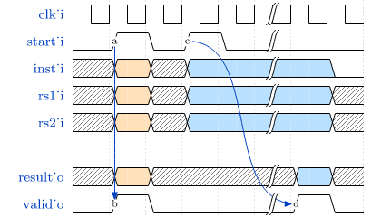
3.7. Control and Status Registers (CSRs)
The following table shows a summary of all available NEORV32 CSRs. The address field defines the CSR address for
the CSR access instructions. The "Name [ASM]" column provides the CSR name aliases that can be used in (inline) assembly.
The "Name [C]" column lists the name aliases that are defined by the NEORV32 core library. These can be used in plain C code.
The "Access" column shows the minimal required privilege mode required for accessing the according CSR (M = machine-mode,
U = user-mode, D = debug-mode) and the read/write capabilities (RW = read-write, RO = read-only)
|
Unused, Reserved, Unimplemented and Disabled CSRs
All CSRs and CSR bits that are not listed in the table below are unimplemented and are hardwired to zero. Additionally,
CSRs that are unavailable ("disabled") because the according ISA extension is not enabled are also considered unimplemented
and are also hardwired to zero. Any access to such a CSR will raise an illegal instruction exception. All writable CSRs provide
WARL behavior (write all values; read only legal values). Application software should always read back a CSR after writing
to check if the targeted bits can actually be modified.
|
| Address | Name [ASM] | Name [C] | Access | Description |
|---|---|---|---|---|
0x001 |
|
URW |
Floating-point accrued exceptions |
|
0x002 |
|
URW |
Floating-point dynamic rounding mode |
|
0x003 |
|
URW |
Floating-point control and status |
|
0x300 |
|
MRW |
Machine status register - low word |
|
0x301 |
|
MRW |
Machine CPU ISA and extensions |
|
0x304 |
|
MRW |
Machine interrupt enable register |
|
0x305 |
|
MRW |
Machine trap-handler base address for ALL traps |
|
0x306 |
|
MRW |
Machine counter-enable register |
|
0x310 |
|
MRW |
Machine status register - high word |
|
0x30a |
|
MRW |
Machine environment configuration register - low word |
|
0x31a |
|
MRW |
Machine environment configuration register - high word |
|
0x320 |
|
MRW |
Machine counter-inhibit register |
|
0x321 |
|
MRW |
Machine cycle counter privilege mode filtering - low word |
|
0x322 |
|
MRW |
Machine instret counter privilege mode filtering - low word |
|
0x721 |
|
MRW |
Machine cycle counter privilege mode filtering - high word |
|
0x722 |
|
MRW |
Machine instret counter privilege mode filtering - high word |
|
0x340 |
|
MRW |
Machine scratch register |
|
0x341 |
|
MRW |
Machine exception program counter |
|
0x342 |
|
MRW |
Machine trap cause |
|
0x343 |
|
MRW |
Machine trap value |
|
0x344 |
|
MRW |
Machine interrupt pending register |
|
0x3a0 .. 0x303 |
|
MRW |
Physical memory protection configuration registers |
|
0x3b0 .. 0x3bf |
|
MRW |
Physical memory protection address registers |
|
0x7a0 |
|
MRW |
Trigger select register |
|
0x7a1 |
|
MRW |
Trigger data register 1 |
|
0x7a2 |
|
MRW |
Trigger data register 2 |
|
0x7a4 |
|
MRW |
Trigger information register |
|
0x7b0 |
|
DRW |
Debug control and status register |
|
0x7b1 |
|
DRW |
Debug program counter |
|
0x7b2 |
|
DRW |
Debug scratch register 0 |
|
0xb00 |
|
MRW |
Machine cycle counter low word |
|
0xb02 |
|
MRW |
Machine instruction-retired counter low word |
|
0xb80 |
|
MRW |
Machine cycle counter high word |
|
0xb82 |
|
MRW |
Machine instruction-retired counter high word |
|
0xc00 |
|
URO |
Cycle counter low word |
|
0xc01 |
|
URO |
System time low word |
|
0xc02 |
|
URO |
Instruction-retired counter low word |
|
0xc80 |
|
URO |
Cycle counter high word |
|
0xc81 |
|
URO |
System time high word |
|
0xc82 |
|
URO |
Instruction-retired counter high word |
|
0x323 .. 0x33f |
|
MRW |
Machine performance-monitoring event select |
|
0xb03 .. 0xb1f |
|
MRW |
Machine performance-monitoring counter low word |
|
0xb83 .. 0xb9f |
|
MRW |
Machine performance-monitoring counter high word |
|
0xc03 .. 0xc1f |
|
URO |
Performance-monitoring counter low word |
|
0xc83 .. 0xc9f |
|
URO |
Performance-monitoring counter high word |
|
0xf11 |
|
MRO |
Machine vendor ID |
|
0xf12 |
|
MRO |
Machine architecture ID |
|
0xf13 |
|
MRO |
Machine implementation ID / version |
|
0xf14 |
|
MRO |
Machine hardware thread ID |
|
0xf15 |
|
MRO |
Machine configuration pointer register |
|
0xfc0 |
|
MRO |
Extended machine CPU ISA and extensions low word |
|
0xfc1 |
|
MRO |
Extended machine CPU ISA and extensions high word |
|
3.7.1. Floating-Point CSRs
fflags
Name |
Floating-point accrued exceptions |
Address |
|
Reset value |
|
ISA |
|
Description |
FPU status flags. |
| Bit | R/W | Function |
|---|---|---|
4 |
r/w |
NV: invalid operation |
3 |
r/w |
DZ: division by zero |
2 |
r/w |
OF: overflow |
1 |
r/w |
UF: underflow |
0 |
r/w |
NX: inexact |
frm
Name |
Floating-point dynamic rounding mode |
Address |
|
Reset value |
|
ISA |
|
Description |
The |
| Bit | R/W | Function |
|---|---|---|
2:0 |
r/w |
Rounding mode |
fcsr
Name |
Floating-point control and status register |
Address |
|
Reset value |
|
ISA |
|
Description |
The |
| Bit | R/W | Function |
|---|---|---|
7:5 |
r/w |
Rounding mode ( |
4:0 |
r/w |
Accrued exception flags ( |
3.7.2. Machine Trap Setup CSRs
mstatus
Name |
Machine status register - low word |
Address |
|
Reset value |
|
ISA |
|
Description |
The |
| Bit | Name [C] | R/W | Function |
|---|---|---|---|
21 |
|
r/w |
TW: Trap on execution of |
17 |
|
r/w |
MPRV: Effective privilege mode for load/stores; use |
12:11 |
|
r/w |
MPP: Previous machine privilege mode, |
7 |
|
r/w |
MPIE: Previous machine-mode interrupt enable flag state |
3 |
|
r/w |
MIE: Machine-mode interrupt enable flag |
misa
Name |
ISA and extensions |
Address |
|
Reset value |
|
ISA |
|
Description |
The |
The NEORV32 misa CSR is read-only. Hence, active CPU extensions are entirely defined by pre-synthesis configurations
and cannot be switched on/off during runtime. For compatibility reasons any write access to this CSR is simply ignored and
will not cause an illegal instruction exception.
|
| Bit | Name [C] | R/W | Function |
|---|---|---|---|
31:30 |
|
r/- |
MXL: 32-bit architecture indicator (always |
23 |
|
r/- |
X: bit is always set to indicate non-standard / NEORV32-specific extensions |
20 |
|
r/- |
U: CPU extension (user mode) available, set when |
12 |
|
r/- |
M: CPU extension (mul/div) available, set when |
8 |
|
r/- |
I: CPU base ISA, cleared when |
4 |
|
r/- |
E: CPU extension (embedded) available, set when |
2 |
|
r/- |
C: CPU extension (compressed instruction) available, set when |
1 |
|
r/- |
B: CPU extension (bit-manipulation) available, set when |
0 |
|
r/- |
A: CPU extension (atomic memory access) available, set when |
Machine-mode software can discover available Z* sub-extensions (like Zicsr or Zfinx) by checking the NEORV32-specific
mxisa[h] CSRs.
|
mie
Name |
Machine interrupt-enable register |
Address |
|
Reset value |
|
ISA |
|
Description |
The |
| Bit | Name [C] | R/W | Function |
|---|---|---|---|
31:16 |
|
r/w |
Fast interrupt channel 15..0 enable |
11 |
|
r/w |
MEIE: Machine external interrupt enable |
7 |
|
r/w |
MTIE: Machine timer interrupt enable (from Core-Local Interruptor (CLINT)) |
3 |
|
r/w |
MSIE: Machine software interrupt enable (from Core-Local Interruptor (CLINT)) |
mtvec
Name |
Machine trap-handler base address |
Address |
|
Reset value |
|
ISA |
|
Description |
The |
| Bit | R/W | Function |
|---|---|---|
31:2 |
r/w |
BASE: in DIRECT mode = 4-byte-aligned base address of trap base handler, all traps jump to |
1:0 |
r/w |
MODE: mode configuration, |
mcounteren
Name |
Machine counter enable |
Address |
|
Reset value |
|
ISA |
|
Description |
The |
| Bit | Name [C] | R/W | Function |
|---|---|---|---|
31:3 |
|
r/w |
HPMn: User-mode is allowed to read according |
2 |
|
r/w |
IR: User-mode is allowed to read |
1 |
|
r/w |
TM: User-mode is allowed to read |
0 |
|
r/w |
CY: User-mode is allowed to read |
mstatush
Name |
Machine status register - high word |
Address |
|
Reset value |
|
ISA |
|
Description |
The features of this CSR are not implemented yet. The register is read-only and always returns zero. |
3.7.3. Machine Trap Handling CSRs
mscratch
Name |
Scratch register for machine trap handlers |
Address |
|
Reset value |
|
ISA |
|
Description |
The |
mepc
Name |
Machine exception program counter |
Address |
|
Reset value |
|
ISA |
|
Description |
The |
mepc[0] is hardwired to zero. If IALIGN = 32 (i.e. C ISA Extension is disabled) then mepc[1] is also hardwired to zero.
|
mcause
Name |
Machine trap cause |
Address |
|
Reset value |
|
ISA |
|
Description |
The |
| Bit | R/W | Function |
|---|---|---|
31 |
r/w |
Interrupt: |
30:5 |
r/- |
Hardwired to zero |
4:0 |
r/w |
Exception code: see NEORV32 Trap Listing |
mtval
Name |
Machine trap value |
Address |
|
Reset value |
|
ISA |
|
Description |
The |
mip
Name |
Machine interrupt pending |
Address |
|
Reset value |
|
ISA |
|
Description |
The |
| Bit | Name [C] | R/W | Function |
|---|---|---|---|
31:16 |
|
r/- |
FIRQxP: Fast interrupt channel 15..0 pending, see NEORV32-Specific Fast Interrupt Requests; cleared by source-specific mechanism |
11 |
|
r/- |
MEIP: Machine external interrupt pending, triggered by |
7 |
|
r/- |
MTIP: Machine timer interrupt pending, triggered by |
3 |
|
r/- |
MSIP: Machine software interrupt pending, triggered by |
|
FIRQ Channel Mapping
See section NEORV32-Specific Fast Interrupt Requests for the mapping of the FIRQ channels and the according
interrupt-triggering processor module.
|
3.7.4. Machine Configuration CSRs
menvcfg
Name |
Machine environment configuration register - low word |
Address |
|
Reset value |
|
ISA |
|
Description |
Currently, the features of this CSR are not supported. Hence, the entire register is hardwired to all-zero. |
menvcfgh
Name |
Machine environment configuration register - high word |
Address |
|
Reset value |
|
ISA |
|
Description |
Currently, the features of this CSR are not supported. Hence, the entire register is hardwired to all-zero. |
3.7.5. Machine Physical Memory Protection CSRs
The physical memory protection system is configured via the PMP_NUM_REGIONS and PMP_MIN_GRANULARITY top entity
generics. PMP_NUM_REGIONS defines the total number of implemented regions. Note that the maximum number of regions
is constrained to 16. If trying to access a PMP-related CSR beyond PMP_NUM_REGIONS (but below PMP configuration/address
register 16) no illegal instruction exception is triggered. The according CSRs are read-only (writes are ignored) and
always return zero. See section Smpmp ISA Extension for more information.
pmpcfg
Name |
Physical memory protection region configuration registers |
Address |
|
|
|
|
|
|
|
Reset value |
all |
ISA |
|
Description |
Configuration of physical memory protection regions. Each region provides an individual 8-bit array in these CSRs.
Note that, depending on |
| Bit | Name [C] | R/W | Function |
|---|---|---|---|
7 |
|
r/w |
L: Lock bit, prevents further write accesses, also enforces access rights in machine-mode, can only be cleared by CPU reset |
4:3 |
|
r/w |
A: Mode configuration ( |
2 |
|
r/w |
X: Execute permission |
1 |
|
r/w |
W: Write permission |
0 |
|
r/w |
R: Read permission |
|
Implemented Modes
In order to reduce the CPU size certain PMP modes (A bits) can be excluded from synthesis.
Use the PMP_TOR_MODE_EN and PMP_NAP_MODE_EN Processor Top Entity - Generics to control
implementation of the according modes.
|
pmpaddr
Name |
Physical memory protection region address registers |
Address |
|
|
|
|
|
|
|
|
|
|
|
|
|
|
|
|
|
|
|
|
|
|
|
|
|
|
|
|
|
|
|
Reset value |
all |
ISA |
|
Description |
Region address/boundaries configuration (address/mask bits |
| Bit | R/W | Description |
|---|---|---|
29:0 |
r/w |
address bits |
31:30 |
r-w |
address bits |
3.7.6. (Machine) Counter and Timer CSRs
|
Instruction Retired Counter Increment
The [m]instret[h] counter always increments when a instruction enters the pipeline’s execute stage no matter
if this instruction is actually going to retire or if it causes an exception.
|
cycle[h]
Name |
Cycle counter |
Address |
|
|
|
Reset value |
|
ISA |
|
Description |
The |
time[h]
Name |
System time counter |
Address |
|
|
|
Reset value |
|
ISA |
|
Description |
The |
instret[h]
Name |
Instructions-retired counter |
Address |
|
|
|
Reset value |
|
ISA |
|
Description |
The |
mcycle[h]
Name |
Machine cycle counter |
Address |
|
|
|
Reset value |
|
ISA |
|
Description |
If not halted via the |
minstret[h]
Name |
Machine instructions-retired counter |
Address |
|
|
|
Reset value |
|
ISA |
|
Description |
If not halted via the |
|
Instruction Retiring
Note that all executed instruction do increment the [m]instret[h] counters even if they do not retire
(e.g. if the instruction causes an exception).
|
3.7.7. Hardware Performance Monitors (HPM) CSRs
The actual number of implemented hardware performance monitors is configured via the HPM_NUM_CNTS top entity generic,
Note that always all 29 HPM counter and configuration registers (mhpmcounter*[h] and mhpmevent*) are accessible, but
only the actually configured ones are implemented as "real" physical registers - the remaining ones will be hardwired to zero.
If trying to access an HPM-related CSR beyond HPM_NUM_CNTS no illegal instruction exception is
triggered. These CSRs are read-only, writes are ignored and reads always return zero.
The total counter width of the HPMs can be configured before synthesis via the HPM_CNT_WIDTH generic (0..64-bit).
If HPM_NUM_CNTS is less than 64, all remaining MSB-aligned bits are hardwired to zero.
mhpmevent
Name |
Machine hardware performance monitor event select |
Address |
|
Reset value |
all |
ISA |
|
Description |
The value in these CSRs define the micro-architectural events that cause an increment of the according |
| Bit | Name [C] | R/W | Event Description |
|---|---|---|---|
8 |
|
r/w |
memory store operation (read-modify-write AMOs are counted as 1x load + 1x store operation) |
7 |
|
r/w |
memory load operation (read-modify-write AMOs are counted as 1x load + 1x store operation) |
6 |
|
r/w |
control flow transfer (jump, taken branch, trap entry/exit) |
5 |
|
r/w |
memory/bus/cache/etc. delay/wait cycle while executing any load or store operation (caused by a data bus wait cycle)) |
4 |
|
r/w |
delay/wait cycle caused by a multi-cycle CPU Arithmetic Logic Unit operation (e.g. bit-serial shift) |
3 |
|
r/w |
instruction dispatch wait cycle (wait for instruction prefetch-buffer refill); caused by a fence instruction, a control flow transfer or a instruction fetch bus wait cycle (e.g. cache miss) |
2 |
|
r/w |
executed 16-bit/compressed ( |
1 |
|
r/w |
executed instruction (16-bit/compressed or 32-bit/uncompressed) |
0 |
|
r/w |
active clock cycle (CPU not in Sleep Mode) |
|
Instruction Retiring ("Retired == Executed")
The CPU HPM/counter logic treats all executed instruction as "retired" even if they raise an exception,
are intercepted by an interrupt, trigger a privilege mode change or were not meant to retire (i.e. claimed by the RISC-V spec.).
|
|
Atomic Memory Access
The read-modify-write instructions of the Zaamo ISA Extension operate as simple load for the CPU hardware.
Hence, they will only trigger HPMCNT_EVENT_LOAD and only once.
|
mhpmcounter[h]
Name |
Machine hardware performance monitor (HPM) counter |
Address |
|
|
|
Reset value |
all |
ISA |
|
Description |
If not halted via the |
hpmcounter[h]
Name |
Hardware performance monitor (HPM) counter |
Address |
|
|
|
Reset value |
all |
ISA |
|
Description |
The |
3.7.8. Machine Counter Setup CSRs
mcountinhibit
Name |
Machine counter-inhibit register |
Address |
|
Reset value |
|
ISA |
|
Description |
Set bit to halt the according counter CSR. |
| Bit | Name [C] | R/W | Description |
|---|---|---|---|
15:3 |
|
r/w |
HPMx: Set to |
2 |
|
r/w |
CY: Set to |
1 |
- |
r/- |
TM: Hardwired to zero as |
0 |
|
r/w |
IR: Set to |
mcyclecfg[h]
Name |
Machine cycle counter privilege mode filtering |
Address |
|
|
|
Reset value |
all |
ISA |
|
Description |
Halt cycle counter when CPU operates in a specific privilege mode.
Note that |
| Bit | Name [C] | R/W | Description |
|---|---|---|---|
30 |
|
r/w |
MINH: Set to |
28 |
|
r/w |
UINH: Set to |
minstretcfg[h]
Name |
Machine instret counter privilege mode filtering |
Address |
|
|
|
Reset value |
all |
ISA |
|
Description |
Halt instruction-retired counter when CPU operates in a specific privilege mode.
Note that |
| Bit | Name [C] | R/W | Description |
|---|---|---|---|
30 |
|
r/w |
MINH: Set to |
28 |
|
r/w |
UINH: Set to |
3.7.9. Machine Information CSRs
mvendorid
Name |
Machine vendor ID |
Address |
|
Reset value |
|
ISA |
|
Description |
This register is hardwired to the value provided by the |
| Bits | R/W | Description |
|---|---|---|
31:7 |
r/- |
JEDEC ID bank |
6:0 |
r/- |
JEDEC ID offset |
marchid
Name |
Machine architecture ID |
Address |
|
Reset value |
|
ISA |
|
Description |
The |
mimpid
Name |
Machine implementation ID |
Address |
|
Reset value |
|
ISA |
|
Description |
The |
mhartid
Name |
Machine hardware thread ID |
Address |
|
Reset value |
|
ISA |
|
Description |
The |
mconfigptr
Name |
Machine configuration pointer register |
Address |
|
Reset value |
|
ISA |
|
Description |
The features of this CSR are not implemented yet. The register is read-only and always returns zero. |
3.7.10. NEORV32-Specific CSRs
|
RISC-V-Compliant Mapping
NEORV32-specific CSRs are mapped to addresses that are explicitly reserved for custom/implementation-specific use.
|
mxisa[h]
Name |
Machine extended ISA and extensions register |
Address |
|
|
|
Reset value |
|
ISA |
|
Description |
The |
| Bit | Name [C] | R/W | Description |
|---|---|---|---|
31 |
|
r/- |
|
30 |
|
r/- |
|
29 |
|
r/- |
|
28 |
|
r/- |
"`C` without floating-point", available when |
27 |
|
r/- |
|
26 |
|
r/- |
|
25 |
|
r/- |
|
24 |
|
r/- |
|
23 |
|
r/- |
|
22 |
|
r/- |
|
21 |
|
r/- |
|
20 |
|
r/- |
|
19 |
|
r/- |
|
18 |
|
r/- |
|
17 |
|
r/- |
|
16 |
|
r/- |
|
15 |
|
r/- |
|
14 |
|
r/- |
|
13 |
|
r/- |
|
12 |
|
r/- |
|
11 |
|
r/- |
|
10 |
|
r/- |
|
9 |
|
r/- |
|
8 |
|
r/- |
|
7 |
|
r/- |
|
6 |
|
r/- |
|
5 |
|
r/- |
|
4 |
|
r/- |
|
3 |
|
r/- |
|
2 |
|
r/- |
|
1 |
|
r/- |
|
0 |
|
r/- |
|
| Bit | Name [C] | R/W | Description |
|---|---|---|---|
31:2 |
- |
r/- |
reserved, read as zero |
1 |
|
r/- |
|
0 |
|
r/- |
|
3.8. Traps, Exceptions and Interrupts
In this document the following terminology is used (derived from the RISC-V trace specification available at https://github.com/riscv-non-isa/riscv-trace-spec):
-
exception: an unusual condition occurring at run time associated (i.e. synchronous) with an instruction in a RISC-V hart
-
interrupt: an external asynchronous event that may cause a RISC-V hart to experience an unexpected transfer of control
-
trap: the transfer of control to a trap handler caused by either an exception or an interrupt
Whenever an exception or interrupt is triggered, the CPU switches to machine-mode (if not already in machine-mode)
and continues operation at the address being stored in the mtvec CSR. The cause of the trap can be determined via the
mcause CSR. A list of all implemented mcause values and the according description can be found below in section
NEORV32 Trap Listing. The address that reflects the current program counter when a trap was taken is stored to
mepc CSR. Additional information regarding the cause of the trap can be retrieved from the mtval CSR.
The traps are prioritized. If several exceptions occur at once only the one with highest priority is triggered while all remaining exceptions are ignored and discarded. If several interrupts trigger at once, the one with highest priority is serviced first while the remaining ones stay pending. After completing the interrupt handler the interrupt with the second highest priority will get serviced and so on until no further interrupts are pending.
|
Interrupts when in User-Mode
If the core is currently operating in less privileged user-mode, interrupts are globally enabled
even if mstatus.mie is cleared.
|
|
Interrupt Signal Requirements
All CPU interrupt request signals are high-active. Once triggered, the interrupt request line should stay high
until it is explicitly acknowledged by a source-specific mechanism (for example by writing to a specific memory-mapped register).
|
|
Instruction Atomicity and Forward-Progress
All instructions execute as atomic operations - interrupts can only trigger between consecutive instructions.
Additionally, if there is a permanent interrupt request, exactly one instruction from the interrupted program will be executed before
another interrupt handler can start. This allows program progress even if there are permanent interrupt requests.
|
3.8.1. Memory Access Exceptions
If a load operation causes any exception, the instruction’s destination register is not written at all. Furthermore, exceptions caused by a misaligned memory address a physical memory protection fault do not trigger a memory access request at all.
For 32-bit-only instructions (= no C extension) the misaligned instruction exception is raised if bit 1 of the fetch
address is set (i.e. not on a 32-bit boundary). If the C extension is implemented there will never be a misaligned
instruction exception at all.
3.8.2. Nested Interrupts
The CPU supports nested interrupt handling in software. It automatically disables interrupts upon entering any trap
handler by clearing mstatus.MIE. Otherwise, further interrupts during the critical part of the handler (i.e.
before saving the context: mcause, mepc, stack frame, etc.) would cause a context loss. However, software can
explicitly enable interrupts again by manually setting mstatus.MIE from within the handler to allow another
interrupt to trigger.
3.8.3. Custom Fast Interrupt Request Lines
As a custom extension, the NEORV32 CPU features 16 fast interrupt request (FIRQ) lines via the firq_i CPU top
entity signals. These interrupts have custom configuration and status flags in the mie and mip CSRs and also
provide custom trap codes in mcause. These FIRQs are reserved for NEORV32 processor-internal usage only.
3.8.4. NEORV32 Trap Listing
The following tables show all traps that are currently supported by the NEORV32 CPU. It also shows the prioritization and the CSR side-effects.
|
FIRQ Mapping
See section NEORV32-Specific Fast Interrupt Requests for the mapping of the FIRQ channels to the according hardware modules.
|
Table Annotations
The "RTE Trap ID" aliases are defined by the NEORV32 core library and can be used in plain C code
when interacting with the pre-defined RTE functions. The mcause, mepc and mtval
columns show the value being written to the according CSRs when a trap is encountered:
-
I-PC - address of intercepted instruction (instruction at this address has not been executed yet and must be executed after the trap handler to maintain program flow)
-
PC - address of instruction that caused the trap (instruction has been executed)
-
ADDR - memory access address that caused the trap
-
INST - the actual instruction word that caused the trap
-
0 - zero
| Priority | mcause |
RTE Trap ID | Cause | mepc |
mtval |
|---|---|---|---|---|---|
Exceptions (synchronous to instruction execution) |
|||||
highest |
|
|
illegal access fault |
PC |
0 |
|
|
illegal instruction |
PC |
INST |
|
|
|
instruction address misaligned |
PC |
ADDR |
|
|
|
environment call from M-mode |
PC |
0 |
|
|
|
environment call from U-mode |
PC |
0 |
|
|
|
software breakpoint / HW trigger |
PC |
0 |
|
|
|
store address misaligned |
PC |
ADDR |
|
|
|
load address misaligned |
PC |
ADDR |
|
|
|
store access fault |
PC |
ADDR |
|
|
|
load access fault |
PC |
ADDR |
|
Interrupts (asynchronous to instruction execution) |
|||||
|
|
fast interrupt request channel 0 |
I-PC |
0 |
|
|
|
fast interrupt request channel 1 |
I-PC |
0 |
|
|
|
fast interrupt request channel 2 |
I-PC |
0 |
|
|
|
fast interrupt request channel 3 |
I-PC |
0 |
|
|
|
fast interrupt request channel 4 |
I-PC |
0 |
|
|
|
fast interrupt request channel 5 |
I-PC |
0 |
|
|
|
fast interrupt request channel 6 |
I-PC |
0 |
|
|
|
fast interrupt request channel 7 |
I-PC |
0 |
|
|
|
fast interrupt request channel 8 |
I-PC |
0 |
|
|
|
fast interrupt request channel 9 |
I-PC |
0 |
|
|
|
fast interrupt request channel 10 |
I-PC |
0 |
|
|
|
fast interrupt request channel 11 |
I-PC |
0 |
|
|
|
fast interrupt request channel 12 |
I-PC |
0 |
|
|
|
fast interrupt request channel 13 |
I-PC |
0 |
|
|
|
fast interrupt request channel 14 |
I-PC |
0 |
|
|
|
fast interrupt request channel 15 |
I-PC |
0 |
|
|
|
machine external interrupt (MEI) |
I-PC |
0 |
|
|
|
machine software interrupt (MSI) |
I-PC |
0 |
|
lowest |
|
|
machine timer interrupt (MTI) |
I-PC |
0 |
| Trap ID [C] | Triggered when … |
|---|---|
|
bus timeout, bus access error or PMP rule violation during instruction fetch |
|
trying to execute an invalid instruction word (malformed or not supported) or on a privilege violation |
|
fetching a 32-bit instruction word that is not 32-bit-aligned (see note below) |
|
executing |
|
executing |
|
executing |
|
storing data to an address that is not naturally aligned to the data size (half/word) |
|
loading data from an address that is not naturally aligned to the data size (half/word) |
|
bus timeout, bus access error or PMP rule violation during store data operation |
|
bus timeout, bus access error or PMP rule violation during load data operation |
|
caused by interrupt-condition of processor-internal modules, see NEORV32-Specific Fast Interrupt Requests |
|
machine external interrupt (via dedicated Processor Top Entity - Signals) |
|
machine software interrupt (internal Core-Local Interruptor (CLINT) or via dedicated Processor Top Entity - Signals) |
|
machine timer interrupt (internal Core-Local Interruptor (CLINT) or via dedicated Processor Top Entity - Signals) |
|
Resumable Exceptions
Note that not all exceptions are resumable. The "instruction access fault"
and the "instruction address misaligned" exceptions are not resumable in most cases.
|
3.9. Dual-Core Configuration
|
Dual-Core Example Programs
A set of rather simple dual-core example programs can be found in sw/example/demo_dual_core*.
|
Optionally, the CPU core can be implemented as symmetric multiprocessing (SMP) dual-core system.
This dual-core configuration is enabled by the DUAL_CORE_EN top generic.
When enabled, two core complexes are implemented. Each core complex consists of a CPU core and optional
instruction (I$) and data (D$) caches. Similar to the single-core Bus System, the instruction and
data interfaces are switched into a single bus interface by a prioritizing bus switch. The bus interfaces
of both core complexes are further switched into a single system bus using a round-robin arbiter.
Both CPU cores are fully identical and use the same ISA, tuning and cache configurations provided by the
according top generics. However, each core can be identified by the
according "hart ID" that can be retrieved from the mhartid CSR. CPU core 0 (the primary core) has
mhartid = 0 while core 1 (the secondary core) has mhartid = 1.
The following table summarizes the most important aspects when using the dual-core configuration.
CPU configuration |
Both cores use the same cache, CPU and ISA configuration provided by the according top generics. |
Debugging |
A special SMP openOCD script ( |
Clock and reset |
Both cores use the same global processor clock and reset. |
Address space |
Both cores have full access to the same physical Address Space. |
Interrupts |
All Processor Interrupts are routed to both cores. Hence, each core has access to
all NEORV32-Specific Fast Interrupt Requests (FIRQs). Additionally, the RISC-V machine-level external interrupt
(via the top |
RTE |
The NEORV32 Runtime Environment can be used for both cores. However, the RTE needs to be
explicitly initialized on each core (executing |
Memory |
Each core has its own stack. The top of stack of core 0 is defined by the Linker Script
while the top of stack of core 1 has to be explicitly defined by core 0 (see Dual-Core Boot). Both
cores share the same heap, |
Constructors and destructors |
Constructors and destructors are supported by core 0 only (see section C Standard Library). |
Cache layout |
If enabled, each CPU core has its own data and/or instruction cache. |
Cache coherency |
Be aware that there is no cache snooping available. If any CPU1 cache is enabled
care must be taken to prevent access to outdated data - either by using cache synchronization ( |
Bootloader |
Only core 0 will boot and execute the bootloader while core 1 is held in standby. |
Booting |
See section Dual-Core Boot. |
3.9.1. Dual-Core Boot
After reset, both cores start booting at the same reset vector using the same executable. However, core 1 will - regardless of the Boot Configuration - always enter Sleep Mode right inside the default Start-Up Code (crt0). The primary core (core 0) will continue booting, executing either the Bootloader or the pre-installed image from the internal instruction memory (depending on the boot configuration). To explicitly boot-up core 1, the primary core has to use a special library function provided by the NEORV32 software framework:
int neorv32_smp_launch(int (*entry_point)(void), uint8_t* stack_memory, size_t stack_size_bytes);|
Core 1 Boot-Up
Core 0 will ensure that core 1 only uses start-up code from the shared executable.
See https://github.com/stnolting/neorv32/pull/1450.
|
Core 0 uses the two 32-bit MTIMECMP registers of the Core-Local Interruptor (CLINT) to submit a
launch configuration to core 1. This launch configuration consists of the stack layout (via the
stack_memory and stack_size_bytes arguments) and the actual entry point for core 1. When these
registers have been populated, core 0 will trigger the software interrupt of core 1 (also via the CLINT)
to wake it from sleep mode. After that, core 1 will fetch the launch configuration and will start
execution at the configured entry point.
int core1_main(void) { // return `int`, no arguments
  return 0; // return to crt0 and go to sleep mode
}|
Core 1 Stack Memory
The memory for the stack of core 1 (stack_memory) can be either statically allocated (i.e. a global
volatile memory array; placed in the .data or .bss section of core 0) or dynamically allocated
(using malloc; placed on the heap of core 0). In any case the memory should be aligned to a 16-byte
boundary.
|
4. Software Framework
The NEORV32 project comes with a complete software ecosystem called the "software framework" which is based on the C-language RISC-V GCC port and consists of the following parts:
|
Software Documentation
All core libraries and example programs are documented in-code using Doxygen.
The API documentation is automatically built and deployed to GitHub pages:
https://stnolting.github.io/neorv32/sw/files.html.
|
|
Example Programs
A collection of annotated example programs illustrating how to use certain NEORV32 functions
and peripheral/IO modules can be found in sw/example.
|
4.1. Compiler Toolchain
The toolchain for this project is based on the free and open RISC-V GCC-port. You can find the compiler sources and build instructions in the official RISC-V GNU toolchain GitHub repository: https://github.com/riscv-collab/riscv-gnu-toolchain.
|
Toolchain Installation
More information regarding the toolchain (building from scratch or downloading prebuilt ones) can be found in the
user guide section Software Toolchain Setup.
|
4.2. Core Libraries
The NEORV32 project provides a set of pre-defined C libraries that allow an easy integration of the processor/CPU features
(also called "HAL" - hardware abstraction layer). All driver and runtime-related files are located in
sw/lib. These library files are automatically included and linked by adding the following include statement:
#include <neorv32.h> // NEORV32 HAL, core and runtime librariesThe NEORV32 HAL consists of the following files.
| C source file | C header file | Description |
|---|---|---|
- |
|
Main NEORV32 library file |
|
|
General auxiliary/helper function |
|
|
|
|
|
|
|
|
|
|
Control and Status Registers (CSRs) definitions |
|
|
|
|
|
|
|
|
|
|
- |
|
Macros for intrinsics and custom instructions |
- |
|
Legacy / backwards-compatibility wrappers (do not use for new designs) |
|
|
|
|
|
|
|
|
|
|
|
|
|
|
|
|
|
|
|
|
HAL for the SMP Dual-Core Configuration |
|
|
|
|
||
|
|
|
|
|
|
|
|
|
|
|
|
|
|
Primary Universal Asynchronous Receiver and Transmitter (UART0) and UART1 HAL |
|
|
|
|
- |
Platform-specific system calls for newlib |
|
Doxygen API Documentation
The Doxygen-based documentation of all core libraries is available online at
https://stnolting.github.io/neorv32/sw/files.html.
|
4.3. System View Description File (SVD)
A CMSIS-SVD-compatible System View Description (SVD) file including all peripherals is available in sw/svd.
4.4. Application Makefile
Application compilation is based on a centralized GNU makefile (sw/common/common.mk). Each software project
(for example the ones in sw/example folder) should provide a local makefile that just includes the central makefile:
# Set path to NEORV32 root directory
NEORV32_HOME ?= ../../..
# Include the main NEORV32 makefile
include $(NEORV32_HOME)/sw/common/common.mk
Thus, the functionality of the central makefile (including all targets) becomes available for the project. A project-local makefile should be used to define all setup-relevant configuration options instead of changing the central makefile to keep the code base clean. Setting variables in the project-local makefile will override the default configuration. Most example projects already provide a makefile that list all relevant configuration options.
The following example shows the configuration of a local Makefile:
# Override the default CPU ISA
MARCH = rv32imc_zicsr_zifencei

# Override the default RISC-V GCC prefix
RISCV_PREFIX ?= riscv-none-elf-

# Override default optimization goal
EFFORT = -Os

# Add extended debug symbols for Eclipse
USER_FLAGS += -ggdb -gdwarf-3

# Additional sources
APP_SRC += $(wildcard ./*.c)
APP_INC += -I .

# Adjust processor IMEM size and base address
USER_FLAGS += -Wl,--defsym,__neorv32_rom_size=16k
USER_FLAGS += -Wl,--defsym,__neorv32_rom_base=0x00000000

# Adjust processor DMEM size and base address
USER_FLAGS += -Wl,--defsym,__neorv32_ram_size=8k
USER_FLAGS += -Wl,--defsym,__neorv32_ram_base=0x80000000

# Adjust maximum heap size
USER_FLAGS += -Wl,--defsym,__neorv32_heap_size=2k

# Set path to NEORV32 root directory
NEORV32_HOME ?= ../../..

# Include the main NEORV32 makefile
include $(NEORV32_HOME)/sw/common/common.mk
4.4.1. Makefile Targets
Invoking a project-local makefile (executing make or make help) will show the help menu that lists all
available targets as well as all variable including their current setting.
neorv32/sw/example/hello_world$ make
NEORV32 Software Makefile
Find more information at https://github.com/stnolting/neorv32
Use 'make V=1' or set BUILD_VERBOSE to increase build verbosity

Targets:

  help       show this text
  check      check toolchain and list supported ISA extensions
  info       show project/makefile configuration
  gdb        start GNU debugging session
  asm        build and generate <main.asm> assembly listing file
  elf        build and generate <main.elf> ELF file
  exe        build and generate <neorv32_exe.bin> executable file for bootloader upload
  bin        build and generate <neorv32_raw_exe.bin> executable memory image
  hex        build and generate <neorv32_raw_exe.hex> executable memory image
  coe        build and generate <neorv32_raw_exe.coe> executable memory image
  mem        build and generate <neorv32_raw_exe.mem> executable memory image
  mif        build and generate <neorv32_raw_exe.mif> executable memory image
  image      build and generate VHDL IMEM application memory image <neorv32_imem_image.vhd> in local folder
  install    build, generate and install VHDL IMEM application memory image <neorv32_imem_image.vhd>
  clean      clean up project home folder
  clean_all  clean up project home folder and image generator
  all        elf + asm + exe + bin + coe + mem + mif + image + install

Additional targets:

  sim           in-console simulation using default testbench (sim folder) and GHDL
  hdl_lists     regenerate HDL file-lists (*.f) in NEORV32_HOME/rtl
  upload        upload executable to bootloader via UART (/dev/ttyUSB1)
  elf_info      show ELF information
  elf_sections  show ELF sections
  bl_image      build and generate VHDL BOOTROM bootloader memory image <neorv32_bootrom_image.vhd> in local folder
  bootloader    build, generate and install VHDL BOOTROM bootloader memory image <neorv32_bootrom_image.vhd>

Variables:

  BUILD_VERBOSE   Set to increase build verbosity: "0"
  USER_FLAGS      Custom toolchain flags [append only]: "-ggdb -gdwarf-3 -Wl,--defsym,__neorv32_rom_size=16k -Wl,--defsym,__neorv32_rom_base=0x00002000 -Wl,--defsym,__neorv32_ram_size=8k"
  USER_LIBS       Custom libraries [append only]: ""
  EFFORT          Optimization level: "-Os"
  MARCH           Machine architecture: "rv32i_zicsr_zifencei"
  MABI            Machine binary interface: "ilp32"
  APP_INC         C include folder(s) [append only]: "-I ."
  APP_SRC         C source folder(s) [append only]: "./main.c   "
  APP_OBJ         Object file(s) [append only]: ""
  ASM_INC         ASM include folder(s) [append only]: "-I ."
  RISCV_PREFIX    Toolchain prefix: "riscv-none-elf-"
  NEORV32_HOME    NEORV32 home folder: "../../.."
  GDB_ARGS        GDB arguments: "-ex target extended-remote localhost:3333"
  UART_TTY        Serial port for upload to bootloader: "/dev/ttyUSB1"
GHDL_RUN_FLAGS GHDL simulation run arguments: ""|
Build Artifacts
All intermediate build artifacts (like object files and binaries) will be places into a (new) project-local
folder named build. The resulting build artifacts (like executable, the main ELF and all memory
initialization/image files) will be placed in the root project folder.
|
|
Increase Verbosity
Use make V=1 or set BUILD_VERBOSE in your environment to increase build verbosity.
|
|
Compile Flags as C-String
The makefile defines a C string CC_FLAGS_STR that contains all flags passed to the compiler.
This string can be processed at runtime: printf("CC_FLAGS: %s\n", CC_FLAGS_STR);
|
4.4.2. Default Compiler Flags
The central makefile uses specific compiler flags to tune the code to the NEORV32 hardware. Hence, these flags should not be altered. However, experienced users can modify them to further tune compilation.
|
Enable all/extra compiler warnings. |
|
Put functions in independent sections. This allows a code optimization as dead code can be easily removed. |
|
Put data segment in independent sections. This allows a code optimization as unused data can be easily removed. |
|
Use built-in software functions for floating-point divisions and square roots (since the according instructions are not supported yet). |
|
Unaligned memory accesses cannot be resolved by the hardware and require emulation. |
|
Branching is expensive. |
|
Disable floating-point expression contraction (fused multiply-add/sub; not supported by the NEORV32 FPU). |
|
Add (simple) debug information. |
|
Include/link with |
|
Search for the standard C library when linking. |
|
Make sure we have no unresolved references to internal GCC library subroutines. |
|
Do not use the default start code. Instead, the NEORV32-specific start-up code ( |
|
Make the linker perform dead code elimination. |
|
Advanced Debug Symbols
By default, only "simple" symbols are added to the ELF (-g). Extended debug flags (e.g. for Eclipse) can be added
using the USER_FLAGS variable (e.g. USER_FLAGS += -ggdb -gdwarf-3). Note that other debug flags may be required
depending of the GCC/GDB version
|
4.5. Linker Script
The NEORV32-specific linker script (sw/common/neorv32.ld) is used to link the compiled sources according to the
processor’s Address Space). For the final executable, only two memory segments are required:
| Memory section | Description |
|---|---|
|
Instruction memory address space (processor-internal Instruction Memory (IMEM) and/or external memory) |
|
Data memory address space (processor-internal Data Memory (DMEM) and/or external memory) |
These two sections are configured by several variables defined in the linker script and exposed to the build framework (aka the makefile). Those variable allow to customized the RAM/ROM sizes and base addresses. Additionally, a certain amount of the RAM can be reserved for the software-managed heap (see RAM Layout).
| Memory section | Description | Default |
|---|---|---|
|
"ROM" size (instruction memory / IMEM) |
16kB |
|
"RAM" size (data memory / DMEM) |
8kB |
|
"ROM" base address (instruction memory / IMEM) |
|
|
"RAM" base address (data memory / DMEM) |
|
|
Maximum heap size; part of the "RAM" |
0kB |
Each variable provides a default value (e.g. "16K" for the instruction memory /ROM /IMEM size). These defaults can
be overridden by setup-specific values to take the user-defined processor configuration into account (e.g. a different IMEM
size). The USER_FLAGS variable provided by the Application Makefile can also be used to customize the memory
configuration. For example, the following line can be added to a project-specific local makefile to adjust the memory
sizes:
USER_FLAGS += "-Wl,--defsym,__neorv32_rom_size=64k -Wl,--defsym,__neorv32_ram_size=32k"|
Memory Configuration Constraints
Memory sizes have to be a multiple of 4 bytes. Memory base addresses have to be 32-bit-aligned.
|
4.5.1. RAM Layout
The default NEORV32 linker script uses the defined RAM (DMEM) size to map several sections. Note that depending on the application some sections might have zero size.
<End of RAM>
+------------------------------+
|             Stack            |
+------------------------------+
.     stack grows downwards    .
.                              .
.                              .
.      heap grows upwards      .
+------------------------------+
|   Dynamic memory (".heap")   |
+------------------------------+
| Uninitialized data (".bss")  |
+------------------------------+
|  Initialized data (".data")  |
+------------------------------+
<Start of RAM>-
Initialized data (
.data): The data section is placed right at the beginning of the RAM. For example, this contains explicitly initialized global variables which are initialized by the Start-Up Code (crt0). -
Non-initialized data (
.bss): This dynamic data section contains data like global variables without explicit initialization. This memory section is cleared by the Start-Up Code (crt0). -
Heap (
.heap): The heap is used for dynamic memory that is managed by functions likemalloc()andfree(). The heap grows upwards. This section is not initialized at all. -
Stack: The stack starts at the end of the RAM at the last 16-byte aligned address. According to the RISC-V ABI / calling convention the stack is 128-bit-aligned before procedure entry. The stack grows downwards.
|
Heap Size
The maximum size of the heap is defined by the __neorv32_heap_size variable. This variable has to be
explicitly defined in order to define a heap size (and to use dynamic memory allocation at all).
|
|
Heap-Stack Collision
Take care when using dynamic memory to avoid collision of the heap and stack memory areas. There is no compile-time
protection mechanism available as the actual heap and stack size are defined by runtime data.
The physical memory protection extension can be used to implement a guarding mechanism.
|
4.5.2. ROM Layout
The default NEORV32 linker script uses the defined ROM (IMEM) size to map several sections into an executable layout. Note that depending on the application some sections might have zero size.
<End of ROM>
+-----------------------------+
|  Initial data for ".data"   |
+-----------------------------+
|  Read-only data ".rodata"   |
+-----------------------------+
|    Program code ".text"     |
+-----------------------------+
<Start of ROM>-
Program code (
.text): This section contains the actual instructions of the program. -
Read-only data (
.rodata): Read-only data, for example for constants and strings. -
Heap (
.heap): Initialization data that is copied at runtime to the RAM’sdatasection by by the Start-Up Code (crt0).
|
Binary Executable Image
The above sections are concatenated by the Application Makefile to create a standalone and portable executable.
This can be exported in various Executable Image Formats, e.g. for transfer via the Bootloader or to initialize
read-only memory.
|
4.6. C Standard Library
The default software framework relies on newlib as default C standard library. Newlib provides hooks for common
"system calls" (like file handling and standard input/output) that are used by other C libraries like stdio.
These hooks are available in sw/lib/source/newlib.c and were adapted for the NEORV32 processor.
|
Standard Input/Output Streams / Consoles
The UART0
is used to implement all the standard input, output and error consoles (STDIN = file number 0, STDOUT = file
number 1, STDERR = file number 2). All other input/output streams (other file number than 0,1,2) are redirected
to UART1.
|
|
Constructors and Destructors
Constructors and destructors for plain C code or for C++ applications are supported by the software framework.
See sw/example/hello_cpp for a minimal example. Note that constructor and destructors are only executed
by core 0 (primary core) in the SMP Dual-Core Configuration.
|
|
Newlib Test/Demo Program
A simple test and demo program that uses some of newlib’s system functions (like malloc/free and read/write)
is available in sw/example/demo_newlib.
|
|
Executing System Functions on a Host Computer
The NEORV32 on-chip debugger supports Semihosting which allow to use the input/output facilities on a host computer.
|
4.7. Start-Up Code (crt0)
The CPU and also the processor require a minimal start-up and initialization code to bring the hardware into an
operational state. Furthermore, the C runtime requires an initialization before compiled code can be executed.
This setup is done by the start-up code (sw/common/crt0.S) which is automatically linked with every application
program and gets mapped before the actual application code so it gets executed right after boot.
The crt0.S start-up performs the following operations:
CPU 0 (primary core) |
CPU 1 (secondary core) |
setup the stack pointer ( |
|
initialize |
|
install an endless loop as trap handler ("crt0 panic") to |
|
clear |
|
initialize all integer register |
|
initialize |
wait in SMP sleep mode for Dual-Core Boot. |
clear |
|
call constructors |
|
call core0’s |
call core1’s |
execute application |
|
|
|
clear |
|
reinstall an endless loop as trap handler ("crt0 panic") to |
|
|
|
call destructors |
|
execute |
|
halt: CPU enters sleep mode executing |
|
CPU 0 (primary core) |
CPU 1 (secondary core) |
4.8. Executable Image Formats
The Application Makefile generates a flattened binrary from the final ELF file, which is further processed
by the NEORV32 executable image generator (sw/image_gen). This utility tool can generate various types of standalone
and portable executable file formats, which are used, for example, for uploading via the Bootloader or for
initializing SoC ROM modules.
neorv32/sw/image_gen$ ./image_gen
NEORV32 executable image generator

Usage:    image_gen [options]
Example:  image_gen -i elf.bin -o main_exe.bin -b A0000000 -t exe

Options:
  -h            Show this help text and exit
  -i file_name  Flattened binary input file
  -o file_name  Image output file
  -t format     Image output format
  -b address    Bootloader exe base address (hex; for "-t exe" only)

Image formats (using little-Endian byte ordering):
  exe  Executable for bootloader upload (binary file with header)
  vhd  VHDL memory image (raw executable)
  bin  Binary file (raw executable)
  hex  Plain hexdump file (raw executable)
  coe  COE file (8x hex per line, ASCII, raw executable)
  mem  MEM file (8x hex per line, ASCII, raw executable)
  mif  MIF file (8x hex per line, ASCII, raw executable)
The image generator can be used as a stand-alone program, but it is also integrated into the application makefile. This provides corresponding Makefile Targets) for the different image types:
|
Generates an executable binary file (including a header; see Bootloader Image Format) for upload via the Bootloader. |
|
Generates a raw VHDL memory image (package file, package name is the same as the output file name). |
|
Generates a raw binary file for custom purpose. |
|
Generates a raw HEX file for custom purpose (like memory initialization via |
|
Generates a raw COE file for FPGA memory initialization. |
|
Generates a raw MEM file for FPGA memory initialization. |
|
Generates a raw MIF file for FPGA memory initialization. |
|
Image Generator Compilation
The sources of the image generator are automatically compiled when invoking the according makefile targets.
Note that compiling the image generator requires a native C compiler.
|
|
VHDL Memory Initialization Files
The generated VHDL images are plain VHDL packages providing program data as constant array.
Note that this array is always extended to a power of 2. Unused elements are set to zero.
|
4.9. Bootloader
The NEORV32 bootloader provides an optional built-in firmware that allows to upload new application firmware at
any time without the need to re-synthesize the FPGA’s bitstream. The bootloader is automatically executed after
reset when enabled via the Boot Configuration BOOT_MODE_SELECT generic. The bootloader provides the
following key features:
-
interactive user console via UART
-
upload executable via UART
-
load executable from SPI flash; store executable to SPI flash
-
load executable from TWI flash; store executable to TWI flash (option disabled by default)
-
load executable from SD card (option disabled by default)
-
automatic boot sequence: automatically boot from TWI/SPI flash / SD card
-
highly configurable to adapt to application requirements
|
Pre-Built Bootloader Image
This section refers to the default NEORV32 bootloader. The Bootloader ROM (BOOTROM) image file
already contains the pre-compiled bootloader (sw/bootloader/bootloader.c) in its default configuration.
|
|
Minimal Hardware Requirements
The default bootloader image was compiled for a minimal rv32e_zicsr_zifencei ISA configuration and requires a
RAM (DMEM) size of at least 256 bytes. These constraints ensure that the bootloader can be executed on any
CPU/processor configuration. It is recommended to enable at least
UART0,
the CLINT and the GPIO controller.
See Customizing the Internal Bootloader for more information.
|
4.9.1. Bootloader Console
The default bootloader provides a serial console via UART0 for user interaction using the following terminal settings:
-
19200 Baud, 8 data bits, no parity bit, 1 stop bit (
19200-8-N-1) -
line breaks: carriage return + newline (
\r\n)
|
Terminal Program
Any terminal program that can connect to a serial port should work. However, make sure the program can transfer
data in raw byte mode without any protocol overhead (e.g. XMODEM). Note that some terminal programs struggle
with transmitting files larger than 4kB (see https://github.com/stnolting/neorv32/pull/215).
For Windows I can recommend TeraTerm (GUI) and SimplySerial (Window terminal). For Linux I can recommend picocom.
|
By default the bootloader uses the LSB of the GPIO output port (gpio_o(0)) for a high-active status LED.
If the GPIO’s direction control feature is implemented, only pin 0 is configured as output; the remaining pins
are configured as inputs. All other output pins are set to low. After reset, the status LED will start blinking
at 2Hz and the Auto Boot Sequence is started. This auto-boot sequence can be skipped within 8s by pressing any key.
NEORV32 Bootloader
build: Dec 13 2025 (1)

Auto-boot in 8s. Press any key to abort. (2)
Aborted. (3)

Type 'h' for help.
CMD:> (4)| 1 | Bootloader version (compile date). |
| 2 | Start of auto-boot sequence. |
| 3 | Auto-boot sequence aborted due to user console input. |
| 4 | Command prompt. |
To see a list of all available commands press h to see the help menu:
CMD:> h
Available CMDs:
h: Help                (1)
i: System info         (2)
r: Restart             (3)
u: Upload via UART     (4)
t: TWI flash - load    (5)
w: TWI flash - program (6)
l: SPI flash - load    (7)
s: SPI flash - program (8)
c: SD card - load      (9)
e: Start executable    (10)
x: Exit                (11)
CMD:>| 1 | Show "Available CMDs" help text again. |
| 2 | Show hardware configuration information. |
| 3 | Restart bootloader and auto-boot sequence. |
| 4 | Upload new executable (neorv32_exe.bin) via UART. |
| 5 | Load executable from TWI flash (this option is disabled by default). |
| 6 | Store executable to TWI flash (this option is disabled by default). |
| 7 | Load executable from SPI flash. |
| 8 | Program previously-uploaded executable to SPI flash. |
| 9 | Load executable from SD card (this option is disabled by default). |
| 10 | Start the (up)loaded executable. |
| 11 | Raise a breakpoint exception: If a debugger is connected this will transfer control to the debugger. If no debugger is connected this will print an exception error (Bootloader Error Codes) shutting down the processor. |
|
Unavailable Commands
Note that not all options are enabled in the default bootloader configuration in order to keep the bootloader
ROM size below 4kB. However, these options can be enabled in config.h (see Customizing the Internal Bootloader).
|
Available commands can be executed by typing the according letter. For example, when executing the i command
the general system configuration is printed:
CMD:> i
HWV:  0x01120101 (1)
CLK:  0x05f5e100 (2)
MISA: 0x40901107 (3)
XISA: 0x00000000:0x0fc06fd3 (4)
SOC:  0x38efc87b (5)
MISC: 0x0a010d00 (6)
CMD:>| 1 | Processor hardware version in BCD format (mimpid CSR). |
| 2 | Processor clock speed in Hz (CLK register of System Configuration Information Memory (SYSINFO). |
| 3 | RISC-V CPU extensions (misa CSR). |
| 4 | Additional RISC-V CPU (sub-)extensions (high & low words of mxisa[h] CSRs). |
| 5 | Processor configuration (SOC register of System Configuration Information Memory (SYSINFO). |
| 6 | Miscellaneous memory and SoC configuration (MISC register of System Configuration Information Memory (SYSINFO). |
4.9.2. Bootloader Image Format
In order to keep the bootloader as small as possible, complete ELF parsing was omitted. Therefore, a compiled ELF cannot be loaded directly into the processor via the bootloader. Instead, the image generator (see Executable Image Formats) is used to create a simplified executable file for the bootloader that contains all the necessary information from the ELF and can be processed by the bootloader with little overhead.
After the executable has been compiled, the image generator extracts the relevant sections and combines them into an image that corresponds to the ROM Layout of the processor configuration. This image is preceded by a simple header containing information for transmission as well as for relocation and booting. The header consists of four individual 32-bit words, which, like the actual image, are stored in low-endian byte order.
// bootloader executable header, little-Endian
typedef struct __attribute__((packed,aligned(4))) {
  uint32_t signature; // = 0x214F454E ("NEO!")
  uint32_t base_addr; // executable base address & entry point
  uint32_t size;      // size in bytes
  uint32_t checksum;  // sum-complement checksum
} exe_header_t;
The first word represents the signature (0x214F454E, "NEO!" as string representation). Based on this, the bootloader
can recognize a valid executable that also matches the bootloader version.
The next word defines the base address of the image. The bootloader stores the received image starting at this address.
This allows the bootloader to store different programs at different memory addresses, for example. The base address is
ultimately defined by the Linker Script using the __neorv32_rom_base symbol. This also corresponds to the entry
point of the program that is executed during bootup.
The next word is the size of the image in bytes. The size of the generated executable is always a multiple of 4.
The last word represents a checksum that ensures the transfer and integrity of the executable. To keep the bootloader simple, a simple "sum complement" checksum is used here.
neorv32/sw/example/processor_check$ xxd -e -l 32 neorv32_exe.bin
00000000: 214f454e 00000000 00007078 2af7f9c6   NEO!....xp.....*
4.9.3. Auto Boot Sequence
After reset, the bootloader waits 8 seconds for UART console input before it starts the automatic boot sequence. Depending on the configuration (Customizing the Internal Bootloader) the bootloader will try to fetch a valid executable from different sources:
-
Try to load an executable from TWI flash (default device ID is
0xA0). -
Try to load an executable from SPI flash (default SPI chip select line is
spi_csn_o(0)). -
Try to load file
boot.binfrom SD flash (default SPI chip select line isspi_csn_o(1)).
If a valid boot image is loaded it will be immediately started. If no valid executable can be fetched the interactive bootloader console is started.
4.9.4. Uploading an Executable
-
Connect the primary UART (UART0) interface of the processor to a serial port of your host computer.
-
Start a serial terminal program.
-
Open a connection to the the serial port your UART is connected to.
-
Press the NEORV32 reset button to restart the bootloader. The status LED starts blinking and the bootloader intro screen appears in the console. Press any key to abort the automatic boot sequence and to start the actual bootloader user interface console.
-
Execute the "Upload" command by typing
u. Now the bootloader is waiting for a binary executable to be send:Awaiting neorv32_exe.bin… -
Use the "send file" option of your terminal program to send a valid NEORV32 executable (
neorv32_exe.bin). Make sure the terminal sends the executable in raw binary mode. -
If everything went fine,
Awaiting neorv32_exe.bin… OKis printed in the terminal. -
The executable is now in the instruction memory of the processor. To execute the program right now run the "start executable" command by typing
e.
|
Uploading via
The Application Makefile provides an “upload” target that allows you to transfer a compiled executable directly
to the bootloader via UART right from the console. This script handles the communication with the bootloader and is
based on a simple shell helper script make upload right from the consoleneorv32/sw/image_gen/uart_upload.sh. Example:
neorv32/sw/example/demo_blink_led$ make UART_TTY=/dev/ttyUSB1 upload.
The serial interface device is defined by UART_TTY .
|
|
UART Overflow Detection and Hardware Flow Control
For setups that use very high custom baud rates values and/or provide very high main memory latency (e.g. external
DDR-RAM with several cache layers), it is recommended to enable the UART RTS/CTS hardware flow control. In addition,
enabling overflow detection can make debugging easier. See Customizing the Internal Bootloader for more information.
|
4.9.5. Programming an SPI or TWI Flash
This guide shows how to write an executable to the SPI flash via the bootloader so it can be automatically fetched and executed after processor reset. If the TWI flash option is enabled, an according command for programming the TWI flash is available.
-
Reset the NEORV32 processor and wait until the bootloader start screen appears.
-
Abort the auto boot sequence and start the user console by pressing any key.
-
Press
uto upload the executable that shall be programmed to the flash. -
Send the binary via the terminal program. When the upload is completed and "OK" appears, press
sto trigger the SPI flash programming:
CMD:> u
Awaiting neorv32_exe.bin... OK
CMD:> s
Write 0x00001614 bytes to SPI flash @0x00400000 (y/n)?-
The bootloader shows the size of the executable and the base address of the SPI flash where the executable will be stored. A prompt appears: type
yto start the programming or typento abort.
CMD:> u
Awaiting neorv32_exe.bin... OK
CMD:> s
Write 0x00001614 bytes to SPI flash @0x00400000 (y/n)?
Flashing... OK
CMD:>-
Note that flash programming can take some time (depending on the TWI/SPI clock configuration in
config.h). If "OK" appears, the programming process was successful and the flash can be used for the auto-boot sequence.
4.9.6. Booting from SD Card
The SD card is accessed in SPI mode. The card has to be formatted using the FAT32 file system with
a sector size of at least 512 bytes. The executable has to be placed in the card’s root directory.
By default the bootloader will fetch the boot.bin file, which is just a renamed copy of the
default neorv32_exe.bin file that is generated by the application compilation flow. The name of the
SD card’s boot file can be changed to a custom file name (see Customizing the Internal Bootloader),
but it has to use the 8.3 DOS format (max 8 character for the name plus dot plus 3 characters suffix).
SD-card and FAT32 support is provided by the great Petit FatFs library by Elm-Chan: https://elm-chan.org/fsw/ff/00index_p.html
4.9.7. Customizing the Internal Bootloader
The NEORV32 bootloader provides several options to configure it for a custom setup. It configured via set of
C-language defines in sw/bootloader/config.h. All defines provide default value that can be edited or
overridden by Makefile directives.
| Parameter | Default | Legal values | Description |
|---|---|---|---|
Additional includes |
|||
- |
- |
- |
Add further |
Serial console - requires Primary Universal Asynchronous Receiver and Transmitter (UART0) |
|||
|
|
|
Set to |
|
|
any |
Baud rate of UART0. |
|
|
|
Enable RX overflow detection. Recommended for high baud rates / high memory latency. |
|
|
|
Enable RTS/CTS hardware flow control. Recommended for very high baud rates / high memory latency. |
Status LED - requires General Purpose Input and Output Port (GPIO) |
|||
|
|
|
Enable bootloader status led ("heart beat") at |
|
|
|
|
Auto-boot - requires Core-Local Interruptor (CLINT) |
|||
|
|
|
Auto-boot enabled when |
|
|
any |
Timeout in seconds after which the auto-boot sequence starts (if there is no UART input by the user). |
TWI flash - requires Two-Wire Serial Interface Controller (TWI) |
|||
|
|
|
Set to |
|
|
|
Set to |
|
|
|
TWI clock prescaler. |
|
|
|
TWI clock divider value. |
|
|
any |
8-bit TWI device address (with R/W bit cleared). |
|
|
32-bit |
Defines the TWI flash base address for the executable. |
|
|
|
Number of TWI flash address bytes. |
SPI flash - requires Serial Peripheral Interface Controller (SPI) |
|||
|
|
|
Set to |
|
|
|
Set to |
|
|
|
SPI chip select line (port |
|
|
|
SPI clock prescaler. |
|
|
|
SPI clock divider value. |
|
|
32-bit |
Defines the SPI flash base address for the executable. |
|
|
|
SPI flash address size in number of bytes. |
|
|
any |
Number of SPI flash address bytes. |
SPI SD card - requires Serial Peripheral Interface Controller (SPI) |
|||
|
|
|
Set to |
|
|
|
SPI chip select line (port |
|
|
|
SPI clock prescaler. |
|
|
|
SPI clock divider value. |
|
|
8.3 DOS format |
File name of the boot image. Has to be located in the root directory. |
Branding |
|||
|
|
any string |
Intro text that is shown in the bootloader console. |
|
|
any string |
Name of executable that is shown in the upload menu. |
Custom Code |
|||
|
|
any code |
User-defined initialization code (wrapped in a macro) that is executed right after the bootloader’s hardware initialization. |
Miscellaneous |
|||
|
|
32-bit |
Default base address of executable; can be used to directly execute from main memory. |
4.9.8. Bootloader Error Codes
|
A device-accessing function returned an error code. Make sure that the device is properly connected and that all required processor modules/interface are actually enabled (by the according Processor Top Entity - Generics). This error can also occur if there was an RX overflow on the UART (if overflow detection is enabled). In this case, either UART hardware flow control should be enabled or the baud rate should be reduced; both adjustments require recompiling the bootloader. |
|
The signature that indicates a valid NEORV32 executable of the accessed executable is incorrect. This can be caused by a temporary transmission error or by an invalid or corrupted executable. |
|
The checksum of the loaded executable is incorrect. This can be caused by a temporary transmission error or by an invalid or corrupted executable. |
|
An unexpected exception has occurred. This can be caused by an invalid bootloader configuration (non-available
processor modules, memory layout, …). For debugging purpose the error message will also display the content of the |
4.10. NEORV32 Runtime Environment
The NEORV32 software framework provides a minimal runtime environment ("RTE") that takes care of a stable and safe execution environment by providing a unified interface for handling of all traps (exceptions and interrupts). Once initialized, the RTE provides Default RTE Trap Handlers that catch all possible traps. These default handlers just output a message via UART when a certain trap has been triggered. The default handlers can be overridden by the application code to install application-specific handler functions for each trap.
Using the RTE is optional but highly recommended for bare-metal / non-OS applications. The RTE provides a simple and comfortable way of delegating traps to application-specific handlers while making sure that all traps (even though they are not explicitly used by the application) are handled correctly. Performance-optimized applications or embedded operating systems may not use the RTE at all in order to increase response time.
4.10.1. RTE Operation
The RTE manages the trap-related CSRs of the CPU’s privileged architecture (see Machine Trap Handling CSRs).
It initializes the mtvec CSR in DIRECT mode, which provides the base entry point for all traps. The address
stored to this register defines the address of the first-level trap handler, which is provided by the NEORV32
RTE. Whenever an exception or interrupt is triggered this first-level trap handler is executed.
The first-level handler performs a complete context save, analyzes the source of the trap and calls the according second-level trap handler, which takes care of the actual exception/interrupt handling. The RTE manages an internal look-up table to track the addresses of the according second-level trap handlers.
After the initial RTE setup, each entry in the RTE’s trap handler look-up table is initialized with a Default RTE Trap Handlers. These default handler do not execute any trap-related operations - they just output a debugging message via the primary UART (UART0) (if enabled) to inform the user that a trap has occurred that is not (yet) handled by a proper application-specific trap handler. After sending this message, the RTE tries to resume normal execution by moving on to the next linear instruction.
|
Dual-Core Configuration
The RTE’s internal trap handler look-up table is used globally for both cores. If a core-specific handling is
required, the according user-defined trap handler need to retrieve the core’s ID from mhartid and branch
accordingly.
|
4.10.2. Using the RTE
The NEORV32 runtime environment is part of the default NEORV32 software framework. The links to the according software references are listed below.
neorv32_rte.c |
|
neorv32_rte.h |
The RTE has to be explicitly enabled by calling the according setup function. It is recommended to do this right at the
beginning of the application’s main function. For the SMP Dual-Core Configuration the RTE setup functions has to
be called on each core that wants to use the RTE.
int main() {

  neorv32_rte_setup(); // setup NEORV32 runtime environment

  ...
After setup, all traps will trigger execution of the RTE’s Default RTE Trap Handlers at first. In order to use application-specific trap handlers the default debug handlers can be overridden by installing user-defined ones:
int neorv32_rte_handler_install(uint8_t id, void (*handler)(void));The first argument id defines the "trap ID" (for example a certain interrupt request) that shall be handled by the
user-defined handler. These IDs are defined in sw/lib/include/neorv32_rte.h. However, more convenient device-specific
aliases are also defined in sw/lib/include/neorv32.h. The second argument handler is the actual function that
implements the user-defined trap handler. The custom handler functions must have a specific type without any arguments
and with no return value:
void custom_trap_handler_xyz(void) {

  // handle trap...
}|
Custom Trap Handler Attributes
Do NOT use the interrupt attribute for the application trap handler functions! This would place an mret
instruction at the end of the handler making it impossible to return to the first-level trap handler of the RTE core.
|
mscratch CSRmscratch CSR should not be used inside an application trap handler as this register is used by the RTE to
provide the base address of the application’s stack frame Application Context Handling (i.e. modifying the
registers of application code that caused a trap).
|
The following example shows how to install trap handlers for exemplary traps.
neorv32_rte_handler_install(RTE_TRAP_MTI, machine_timer_irq_handler); // handler for machine timer interrupt
neorv32_rte_handler_install(RTE_TRAP_MENV_CALL, environment_call_handler); // handler for machine environment call exception
neorv32_rte_handler_install(SLINK_RX_RTE_ID, slink_rx_handler); // handler for SLINK receive interrupt
4.10.3. Default RTE Trap Handlers
The default RTE trap handlers are executed when a certain trap is triggered that is not (yet) handled by an
application-defined trap handler. The default handler will output a message giving additional debug information
via the Primary Universal Asynchronous Receiver and Transmitter (UART0) to inform the user and it will also
try to resume normal program execution (exemplary RTE outputs are shown below). The specific message right at
the beginning of the debug trap handler message corresponds to the trap code obtained from the mcause CSR
(see NEORV32 Trap Listing).
In most cases the RTE can successfully continue operation - for example if it catches an interrupt request that is not handled by the actual application program. However, if the RTE catches an un-handled trap like a bus access fault exception, continuing execution will most likely fail making the CPU crash.
<NEORV32-RTE-PANIC> [cpu0|M] Illegal instruction MEPC=0x000002d6 MTVAL=0x000000FF </NEORV32-RTE-PANIC> (1)
<NEORV32-RTE-PANIC> [cpu0|U] Illegal instruction MEPC=0x00000302 MTVAL=0x00000000 </NEORV32-RTE-PANIC> (2)
<NEORV32-RTE-PANIC> [cpu0|U] Load address misaligned MEPC=0x00000440 MTVAL=0x80000101 </NEORV32-RTE-PANIC> (3)
<NEORV32-RTE-PANIC> [cpu1|M] FIRQ channel 0x00000003 MEPC=0x00000820 MTVAL=0x00000000 </NEORV32-RTE-PANIC> (4)
<NEORV32-RTE-PANIC> [cpu1|M] Instruction access fault MEPC=0x90000000 MTVAL=0x00000000 FATAL! HALTING CPU </NEORV32-RTE-PANIC>\n (5)| 1 | Illegal 32-bit instruction MTVAL=0x000000FF at address MEPC=0x000002d6 while CPU 0 was in machine-mode ([cpu0|M]). |
| 2 | Illegal 16-bit instruction MTVAL=0x00000000 at address MEPC=0x00000302 while CPU 0 was in user-mode ([cpu0|U]). |
| 3 | Misaligned load access at address MEPC=0x00000440 (trying to load a full 32-bit word from address MTVAL=0x80000101) while CPU 0 was in user-mode ([cpu0|U]). |
| 4 | Fast interrupt request from channel 3 before executing instruction at address MEPC=0x00000820 while CPU 1 was in machine-mode ([cpu0|M]). |
| 5 | Instruction bus access fault at address MEPC=0x90000000 while CPU 1 was in machine-mode ([cpu0|M]). This is a fatal/non-resumable exception halting the CPU. |
4.10.4. Application Context Handling
Upon trap entry the RTE backups the entire application context (i.e. all x general purpose registers) to the
stack. The context is restored automatically after trap completion. The base address of the according stack frame
is copied to the mscratch CSR. By having this information available, the RTE provides dedicated functions
for accessing and altering the application context:
// Prototypes
uint32_t neorv32_rte_context_get(int x); // read register
void     neorv32_rte_context_put(int x, uint32_t data); // write data to register

// Examples
uint32_t tmp = neorv32_rte_context_get(9); // read register 'x9'
neorv32_rte_context_put(28, tmp); // write 'tmp' to register 'x28'
The x argument is used to specify one of the RISC-V general purpose register x0 to x31. Note that registers
x16 to x31 are not available if the RISC-V E ISA Extension is enabled. For he SMP Dual-Core Configuration
the provided context functions will access the stack frame of the interrupted application code that was running
on the specific CPU core that caused the trap entry.
The context access functions can be used by application-specific trap handlers to emulate unsupported CPU / SoC features like unimplemented IO modules, unsupported instructions and even unaligned memory accesses.
|
Demo Program: Emulate Unaligned Memory Access
A demo program, which showcases how to emulate unaligned memory accesses using the NEORV32 runtime environment
can be found in sw/example/demo_emulate_unaligned.
|
5. On-Chip Debugger (OCD)
The NEORV32 Processor features an on-chip debugger (OCD) compatible to the Minimal RISC-V Debug Specification implementing the execution-based debugging scheme (https://docs.riscv.org/reference/debug/index.html).
The on-chip debugger is implemented if the OCD_EN processor top generic is set
to true. Optionally, up to 16 hardware triggers can be implemented (Sdtrig ISA Extension) to support
hardware-assisted break- and watchpoints. Furthermore, the OCD supports an optional Debug Authentication
module to constrain OCD access to authorized parties.
|
Hands-On Tutorial
A simple example on how to use NEORV32 on-chip debugger in combination with OpenOCD and the GNU debugger is shown in
section Debugging using the On-Chip Debugger
of the User Guide.
|
Section Structure
Key Features
-
standard 4-wire JTAG access port
-
debugging of up to 4 CPU cores ("harts")
-
full control of the CPU: halting, single-stepping and resuming
-
indirect access to all core registers and the entire processor address space (via program buffer)
-
execution of arbitrary programs via the program buffer
-
compatible with upstream OpenOCD and GDB
-
optional trigger module for up to 16 hardware break- and watchpoints
-
optional authentication for advanced security
Configuration Options
| Name | Type | Default | Description |
|---|---|---|---|
|
boolean |
false |
Implement the on-chip debugger and the CPU debug mode. |
|
natural |
0 |
Number of implemented HW triggers (Trigger Module / |
|
boolean |
false |
Implement optional Debug Authentication module. |
|
suv(10:0) |
"00000000000" |
JEDEC ID; continuation codes plus vendor ID (passed to the JTAG Debug Transport Module (DTM)). |
Overview
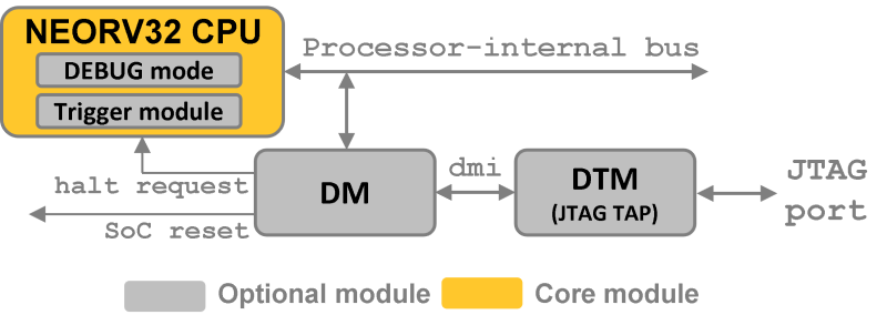
The NEORV32 on-chip debugger is based on five hardware modules:
-
Debug Transport Module (DTM): JTAG access tap to allow an external adapter to interface with the debug module (DM).
-
Debug Module (DM): The RISC-V debug module is the main bridge between the external debugger and the processor being debugged. It provides a data buffer for data transfer from/to the DM, a code ROM containing the "park loop" code, a program buffer to allow the debugger to execute small programs defined by the DM and a status register that is used to communicate exception, halt, resume and execute requests/acknowledges between the debugger and the CPU.
-
Debug Authentication: Authenticator module to secure on-chip debugger access. By default this module implements a very simple authentication mechanism as example. Users can modify/replace this default logic to implement arbitrary authentication mechanism.
-
CPU Debug Mode ISA extension: This ISA extension provides the "debug execution mode" as another CPU operation mode that is used to execute the park loop code from the DM. This mode also provides additional CSRs and instructions.
-
CPU Trigger Module: This module provides up to 16 hardware triggers that can be used as hardware-assisted break- or watchpoints.
Theory of Operation
When debugging the system using the OCD, the external debugger (e.g. GDB) issues a halt request to the CPU to make it enter so-called debug mode. In this mode the application-defined architectural state of the system/CPU is "frozen" so the debugger can monitor it without interfering with the actual application. However, the OCD can also modify the entire architectural state at any time. While in debug mode, the debugger has full control over the entire CPU core.
After halting, the CPU executes the "park loop" code from the code ROM of the debug module (DM). This park loop implements an endless loop that is used to poll a memory-mapped Status Register of the DM. The flags in this register are used to communicate requests from the DM and to acknowledge their processing by the CPU: trigger execution of the program buffer or resume the halted application. Furthermore, the CPU uses this register to signal that the CPU has halted after a halt request or to signal that an exception has been raised while being in debug mode.
5.1. openOCD
By default, the free and open-source openOCD (https://openocd.org/) is used to establish a debugger connection. However, other interfaces can be used (like Segger or Lauterbach tools) if they provide RISC-V support.
openOCD is configured by a set of configuration scripts which are located in neorv32/sw/openocd.
Two top-level scripts are provided: one for the single-core processor configuration (neorv32.cfg)
and another one for the SMP dual-core configuration (neorv32.dual-core.cfg).
Both scripts have the same format and include several helper scripts.
neorv32.cfg)# configuration
set PATH [file dirname [file normalize [info script]]] (1)
set CORENAME neorv32 (2)
set NUMCORES 1 (3)
# configure JTAG interface, setup target, authenticate and start
source [file join $PATH lib/interface.cfg] (4)
source [file join $PATH lib/target.cfg] (5)
source [file join $PATH lib/authenticate.cfg] (6)
source [file join $PATH lib/start.cfg] (7)| 1 | Get the absolute path of the script. |
| 2 | Set the core name that will show up in openOCD and GDB. This can be changed to any custom name. |
| 3 | Number of CPU cores (1 for the single-core setup, 2 for the dual-core setup). |
| 4 | Interface adapter (JTAG) configuration script. Replace by custom adapter setup. |
| 5 | NEORV32-specific target configuration and initialization. |
| 6 | Optional authentication process; the Default Authentication Mechanism is implemented as example; Replace this when using a custom authentication mechanism. |
| 7 | Reset and halt the target. |
5.2. Semihosting
Semihosting is a mechanism developed by ARM that enables code running on the NEORV32 to communicate and use the
input/output facilities on a host computer that is running a debugger. Examples of these facilities include keyboard
input, screen output, and disk I/O. For example, you can use this mechanism to enable functions in the C library,
such as printf() and scanf(), to use the screen and keyboard of the host instead of having a screen and keyboard
on the target system. (source: https://developer.arm.com/documentation/dui0471/i/semihosting/what-is-semihosting-?lang=en)
For example, with semihosting you can
-
print to the host’s
stdoutconsole -
read from the host’s
stdinconsole -
execute arbitrary commands in the host’s shell
-
retrieve the host’s system time
-
read and write files on the host system
-
…
|
Semihosting Example Program
A simple semihosting example program can be found in sw/example/demo_semihosting.
|
The RISC-V semihosting builds upon the ARM standard. Hence, semihosting has to be explicitly enabled on the host
side (in GDB) using the ARM command set:
(gdb) monitor arm semihosting enable
semihosting is enabled
File accesses need to be explicitly enabled. Additionally, the base folder for accessing those files should be defined:
(gdb) monitor arm semihosting_fileio enable
(gdb) monitor arm semihosting_basedir path/to/neorv32/sw/example/demo_semihosting
The NEORV32 software framework provides a build-in library for semihosting primitives (sw/lib/include/neorv32_semihosting.h).
Additionally, accesses to the standard IO streams (stdin and stdout) can be automatically mapped to the host’s console.
Functions such as printf and puts can then print right to the host’s stdout console. Vice versa, functions like scanf
and fgets will read from the host’s stdin. To enable this automatic mapping, the define STDIO_SEMIHOSTING needs to be
defined and the application firmware needs to be recompiled.
stdio.h Calls to Host ComputerUSER_FLAGS += -DSTDIO_SEMIHOSTINGWhen STDIO_SEMIHOSTING is defined all file accesses provided by stdio.h (via Newlib) will be redirected to the host
computer via semihosting services.
|
Redirecting all UART data via Semihosting
You can redirect all physical UART data via semihosting by defining UART_SEMIHOSTING
(e.g. "USER_FLAGS+=-DSTDIO_SEMIHOSTING -DUART_SEMIHOSTING").
|
|
Semihosting Services Without a Host
If any semihosting request is issued without a host being connected, an environment breakpoint exception is raised.
|
Further references:
-
A great overview: https://interrupt.memfault.com/blog/arm-semihosting
-
RISC-V semihosting spec.: https://docs.riscv.org/reference/semihosting/index.html
-
Implementing semihosting on RISC-V: https://embeddedinn.com/articles/tutorial/understanding-riscv-semihosting/
-
Description of the service calls by ARM: https://developer.arm.com/documentation/dui0203/j/semihosting/semihosting-operations?lang=en
5.3. Debug Transport Module (DTM)
The debug transport module "DTM" (VHDL module: rtl/core/neorv32_debug_dtm.vhd) provides a bridge between a standard 4-wire
JTAG test access port ("tap") and the internal debug module interface.
| Name | Width | Direction | Description |
|---|---|---|---|
|
1 |
in |
serial clock |
|
1 |
in |
serial data input |
|
1 |
out |
serial data output |
|
1 |
in |
mode select |
|
Maximum JTAG Clock
All JTAG signals are synchronized to the processor’s clock domain. Hence, no additional clock domain is required
for the DTM. However, this constrains the maximal JTAG clock frequency (jtag_tck_i) to be less than or equal
to 1/5 of the processor clock frequency (clk_i).
|
|
JTAG TAP Reset
The NEORV32 JTAG TAP does not provide a dedicated reset signal ("TRST").
However, JTAG-level resets can be triggered using TMS signaling.
|
|
Maintaining the JTAG Chain
If the on-chip debugger is disabled the JTAG serial input jtag_tdi_i is directly
connected to the JTAG serial output jtag_tdo_o to maintain the JTAG chain.
|
|
JTAG TAP Access via FPGA Vendor Infrastructure
Most FPGAs are programmed via JTAG and also provide mechanisms to access user-defined JTAG logic from within the FPGA
fabric using vendor-specific primitives. Therefore, a dedicated second JTAG connection for the OCD may be omitted.
Instead, the debugger can share the same physical JTAG connection that is already used for FPGA configuration. See the
setups in [neorv32-setups](https://github.com/stnolting/neorv32-setups) for example implementations.
|
The DTM implements a single 5-bit instruction register IR and several data registers DR with different sizes. The
individual data registers are accessed by writing the respective address to the instruction register. The following table
shows all available data registers and their addresses:
Address (via IR) |
Name | Size (bits) | Description |
|---|---|---|---|
|
|
32 |
identification code (see below) |
|
|
32 |
debug transport module control and status register (see below) |
|
|
41 |
debug module interface (see below) |
others |
|
1 |
default JTAG bypass register |
| Bit(s) | Name | R/W | Description |
|---|---|---|---|
31:28 |
|
r/- |
version ID, hardwired to zero |
27:12 |
|
r/- |
part ID, hardwired to zero |
11:1 |
|
r/- |
JEDEC manufacturer ID, assigned via the |
0 |
- |
r/- |
hardwired to |
| Bit(s) | Name | R/W | Description |
|---|---|---|---|
31:21 |
- |
r/- |
reserved, hardwired to zero |
20:18 |
|
r/- |
not implemented; hardwired to zero |
17 |
|
r/w |
setting this bit will reset the debug module interface; this bit auto-clears |
16 |
|
r/w |
setting this bit will clear the sticky error state; this bit auto-clears |
15 |
- |
r/- |
reserved, hardwired to zero |
14:12 |
|
r/- |
recommended idle states (= 0, no idle states required) |
11:10 |
|
r/- |
read-only alias of |
9:4 |
|
r/- |
number of address bits in |
3:0 |
|
r/- |
|
| Bit(s) | Name | R/W | Description |
|---|---|---|---|
40:34 |
|
r/w |
7-bit address, see DM Registers |
33:2 |
|
r/w |
32-bit data to write/read to/from the addressed DM register |
1:0 |
|
r/- |
Read access - status: |
-/w |
Write access - operation: |
5.4. Debug Module (DM)
The debug module "DM" (VHDL module: rtl/core/neorv32_debug_dm.vhd) acts as a translation interface between abstract
operations issued by the debugger application (like GDB) and the platform-specific debugger hardware.
It supports the following features:
-
Gives the debugger necessary information about the implementation.
-
Allows the hart to be halted/resumed/reset and provides the current status.
-
Provides abstract read and write access to the halted hart’s general purpose registers.
-
Provides access to a reset signal that allows debugging from the very first instruction after reset.
-
Provides a program buffer to force the hart to execute arbitrary instructions.
-
Allows memory accesses (to the entire address space) from a hart’s point of view.
-
Optionally implements an authentication mechanism to secure on-chip debugger access.
The NEORV32 DM follows the "Minimal RISC-V External Debug Specification" to provide full debugging capabilities while keeping resource/area requirements at a minimum. It implements the execution based debugging scheme for up to four individual CPU cores ("harts") and provides the following architectural core features:
-
program buffer with 2 entries and an implicit
ebreakinstruction at the end -
indirect bus access via the CPU using the program buffer
-
abstract commands: "access register" plus auto-execution
-
halt-on-reset capability
-
optional authentication
|
DM Spec. Version
The NEORV32 DM complies to the RISC-V DM spec version 1.0.
|
From the DTM’s point of view, the DM implements a set of DM Registers that are used to control and monitor the debugging session. From the CPU’s point of view, the DM implements several memory-mapped registers that are used for communicating data, instructions, debugging control and status (DM CPU Access).
External Reset Output
The entire processor can be reset at any time by the debugger via the ndmreset bit of the dmcontrol register.
This signal is also available as processor top signal (Processor Top Entity - Signals: rstn_ocd_o) and can be used
to reset processor-external modules via the on-chip debugger. This signal is low-active and synchronous to the processor
clock. It is available if the on-chip debugger is actually implemented; otherwise it is hardwired to 1. Note that the
signal also becomes active (low) when the processor’s main reset signal is active (even if the on-chip debugger is
deactivated or disabled for synthesis).
5.4.1. DM Registers
The DM is controlled via a set of registers that are accessed via the DTM. The following registers are implemented:
|
Unimplemented Registers
Write accesses to registers that are not implemented are simply ignored and read accesses to these
registers will always return zero. In both cases no error condition is signaled to the DTM.
|
| Address | Name | Description |
|---|---|---|
0x04 |
Abstract data register 0 |
|
0x10 |
Debug module control |
|
0x11 |
Debug module status |
|
0x12 |
Hart information |
|
0x16 |
Abstract control and status |
|
0x17 |
Abstract command |
|
0x18 |
Abstract command auto-execution |
|
0x1d |
|
Base address of next DM; reads as zero to indicate there is only one DM |
0x20 |
Program buffer 0 |
|
0x21 |
Program buffer 1 |
|
0x30 |
Data to/from the authentication module |
|
0x38 |
|
System bus access control and status; reads as zero to indicate there is no system bus access |
0x40 |
Hart halt summary |
data0
0x04 |
Abstract data 0 |
|
Reset value: |
||
Basic read/write data exchange register to be used with abstract commands (for example to read/write data from/to CPU GPRs). |
||
dmcontrol
0x10 |
Debug module control register |
|
Reset value: |
||
Control of the overall debug module and the hart. The following table shows all implemented bits. All remaining bits/bit-fields are configured as "zero" and are read-only. Writing '1' to these bits/fields will be ignored. |
||
| Bit | Name [RISC-V] | R/W | Description |
|---|---|---|---|
31 |
|
-/w |
set/clear hart halt request |
30 |
|
-/w |
request hart to resume |
28 |
|
-/w |
write |
27 |
- |
r/- |
reserved, hardwired to zero |
26 |
|
r/- |
|
25:16 |
|
r/w |
hart select; only the lowest 3 bits are implemented |
15:6 |
|
r/- |
hardwired to zero |
5:4 |
- |
r/- |
reserved, hardwired to zero |
3 |
|
r/- |
|
2 |
|
r/- |
|
1 |
|
r/w |
put whole system (except OCD) into reset state when |
0 |
|
r/w |
DM enable; writing |
dmstatus
0x11 |
Debug module status register |
|
Reset value: |
||
Current status of the overall debug module and the hart. The entire register is read-only. |
||
| Bit | Name [RISC-V] | Description |
|---|---|---|
31:25 |
reserved |
reserved; zero |
24 |
|
DM in reset state |
23 |
|
|
22 |
|
|
21:20 |
reserved |
reserved; zero |
19 |
|
|
18 |
|
|
17 |
|
|
16 |
|
|
15 |
|
|
14 |
|
|
13 |
|
|
12 |
|
|
11 |
|
|
10 |
|
|
9 |
|
|
8 |
|
|
7 |
|
set if authentication passed; see Debug Authentication |
6 |
|
set if authentication is busy, see Debug Authentication |
5 |
|
|
4 |
|
|
3:0 |
|
|
hartinfo
0x12 |
Hart information |
|
Reset value: see below |
||
This register gives information about the hart. The entire register is read-only. |
||
| Bit | Name [RISC-V] | Description |
|---|---|---|
31:24 |
reserved |
reserved; zero |
23:20 |
|
|
19:17 |
reserved |
reserved; zero |
16 |
|
|
15:12 |
|
|
11:0 |
|
= |
abstracts
0x16 |
Abstract control and status |
|
Reset value: |
||
Command execution info and status. |
||
| Bit | Name [RISC-V] | R/W | Description |
|---|---|---|---|
31:29 |
reserved |
r/- |
reserved; zero |
28:24 |
|
r/- |
|
23:11 |
reserved |
r/- |
reserved; zero |
12 |
|
r/- |
set when a command is being executed |
11 |
|
r/- |
|
10:8 |
|
r/w |
error during command execution (see below); has to be cleared by writing |
7:4 |
reserved |
r/- |
reserved; zero |
3:0 |
|
r/- |
|
Error codes in cmderr (highest priority first):
-
000- no error -
100- command cannot be executed since hart is not in expected state -
011- exception during command execution -
010- unsupported command -
001- invalid DM register read/write while command is/was executing
command
0x17 |
Abstract command |
|
Reset value: |
||
Writing this register will trigger the execution of an abstract command. A new command can only be executed if
|
||
The NEORV32 DM only supports Access Register abstract commands. These commands can only access the
hart’s GPRs x0 - x15/31 (abstract command register index 0x1000 - 0x101f).
|
| Bit | Name [RISC-V] | R/W | Description / required value |
|---|---|---|---|
31:24 |
|
-/w |
|
23 |
reserved |
-/w |
reserved, has to be |
22:20 |
|
-/w |
|
21 |
|
-/w |
|
18 |
|
-/w |
set if the program buffer is executed after the command |
17 |
|
-/w |
set if the operation in |
16 |
|
-/w |
|
15:0 |
|
-/w |
GPR-access only; has to be |
abstractauto
0x18 |
Abstract command auto-execution |
|
Reset value: |
||
Register to configure if a read/write access to a DM register re-triggers execution of the last abstract command. |
||
| Bit | Name [RISC-V] | R/W | Description |
|---|---|---|---|
17 |
|
r/w |
when set reading/writing from/to |
16 |
|
r/w |
when set reading/writing from/to |
0 |
|
r/w |
when set reading/writing from/to |
progbuf
0x20 |
Program buffer 0 |
|
0x21 |
Program buffer 1 |
|
Reset value: |
||
Program buffer (two entries) for the DM. |
||
authdata
0x30 |
Authentication data |
|
Reset value: user-defined |
||
This register serves as a 32-bit serial port to/from the authentication module. See Debug Authentication. |
||
haltsum0
0x40 |
Halt summary 0 |
|
Reset value: |
||
Each bit corresponds to a hart being halted. Only the lowest four bits are implemented. |
||
5.4.2. DM CPU Access
From the CPU’s perspective the DM acts like another memory-mapped peripheral. It occupies 512 bytes of the CPU’s
address space starting at address base_io_dm_c (0xffff0000). This address space is divided into four sections
with 64 bytes each to provide access to the park loop code ROM, the program buffer, the data buffer and the
status register. The program buffer, the data buffer and the status register do not fully occupy the 64-byte-wide
sections and are mirrored several times across the according section.
| Base address | Physical size | Description |
|---|---|---|
|
64 bytes |
ROM for the "park loop" code (Code ROM) |
|
16 bytes |
Program buffer ( |
|
4 bytes |
Data buffer ( |
|
4 bytes |
|
DM Register Access
All memory-mapped registers of the DM can only be accessed by the CPU when in debug mode. Hence, the DM registers are
not accessible for normal CPU operations. Any CPU access outside of debug mode will raise a bus access fault exception.
|
Code ROM
The code ROM contains the minimal OCD firmware that implements the debugger’s park loop.
|
Park Loop Code Sources ("OCD Firmware")
The assembly sources of the park loop code are available in sw/ocd-firmware/park_loop.S.
|
The park loop code provides two entry points where code execution can start. These are used to enter the park loop either when an explicit debug-entry/halt request has been issued (for example a halt request) or when an exception has occurred while executing code in debug mode (from the profram buffer).
| Address | Description |
|---|---|
|
Exception entry address |
|
Normal entry address (halt request) |
When the CPU enters (via an explicit halt request from the debugger) or re-enters debug mode (for example via an
ebreak in the DM’s program buffer), it jumps to the normal entry point that is configured via the
CPU_DEBUG_PARK_ADDR CPU generic. By default, this address is set to dm_park_entry_c,
which is defined in the main package file. If an exception is encountered during debug mode, the CPU jumps to the
address of the exception entry point configured via the CPU_DEBUG_EXC_ADDR CPU
generic. By default, this address is set to dm_exc_entry_c, which is also defined in the main package file.
Status Register
The status register provides a direct communication channel between a CPU executing the park loop and the debugger-controlled DM. This register is used to communicate requests which are issued by the DM, and the according acknowledges which are issued by a CPU core.
From the CPU side the register is accessed using byte-wide load and store operations. Each of the four bytes is associated to a specific request when read or to an according acknowledge when written.

If the park-loop code of a CPU reads a non-zero value from RES then it is requested to resume operation.
If it reads a non-zero value from EXE then it is requested to execute the program buffer.
Accordingly, the park-loop code acknowledges these requests by writing any value (including zero) to the
according byte. The HLT and EXC bytes are used to acknowledge the external halt request and to indicate
that executing the program buffer has encountered an exception, respectively.
| Name | Bits | CPU Read Access (Request) | CPU Write Access (Acknowledge) |
|---|---|---|---|
|
|
- |
CPU has encountered an exception |
|
|
DM requests program buffer execution |
CPU has started to execute program buffer |
|
|
DM requests resuming |
CPU has started to resume |
|
|
- |
CPU has halted |
In the SMP Dual-Core Configuration all cores use the same request/acknowledge communication mechanism by reading and writing the DM status register. The CPU-specific requests and acknowledges can still be clearly assigned, as the CPU Bus Interface implicitly transmits the ID of the accessing CPU core. Therefore, CPU core i only sees the requests intended for it and can only set the acknowledges originating from itself when accessing the DM status register.
5.5. Debug Authentication
Optionally, the on-chip debugger DM can be equipped with an authenticator module to secure debugger access. This authentication
is enabled by the OCD_AUTHENTICATION top generic. When disabled, the debugger is always
authorized and has unlimited access. When enabled, the debugger is required to authenticate in order to gain access.
The authenticator module is implemented as individual RTL module (rtl/core/neorv32_debug_auth.vhd). By default, it implements
a very simple authentication mechanism. Note that this default mechanism is not secure in any way - it is intended as example
logic to illustrate the interface and authentication process. Users can modify the default logic or replace the entire module
to implement a more sophisticated custom authentication mechanism.
The authentication interface is compliant to the RISC-V debug spec and is based on a single CSR and two additional status bits:
-
authdataCSR: this 32-bit register is used to read/write data from/to the authentication module. It is hardwired to all-zero if authentication is not implemented. -
dmstatusCSR:-
The
authenticatedbit (read-only) is set if authentication was successful. The debugger can access the processor only if this bit is set. It is automatically hardwired to1(always authenticated) if the authentication module is not implemented. -
The
authbusybit (read-only) indicates if the authentication module is busy. When set, no data should be written/read to/fromauthdata. This bit is automatically hardwired to0(never busy) if the authentication module is not implemented.
-
openOCD provides dedicated commands to exchange data with the authenticator module:
riscv authdata_read        // read 32-bit from authdata CSR
riscv authdata_write value // write 32-bit value to authdata CSR
Based on these two primitives arbitrary complex authentication mechanism can be implemented.
5.5.1. Default Authentication Mechanism
| The default authentication mechanism is not secure at all. Replace it by a custom design. |
The default authenticator hardware implements a very simple authentication mechanism: a single read/write bit is implemented
that directly corresponds to the authenticated bit in dmstatus. This bit can be read/written as bit zero (LSB) of the
authdata CSR. Writing 1 to this register will result in a successful authentication.
The default openOCD configuration script provides a helper script for authentication. This script also provides several helper functions for interaction with the RISC-V debug mechanism. Additionally, the default authentication mechanism is implemented there (as example):
sw/openocd/authentication.cfg)# read challenge
set CHALLENGE [authenticator_read]
# compute response (default authenticator module)
set RESPONSE [expr {$CHALLENGE | 1}]
# send response
authenticator_write $RESPONSE
# success?
authenticator_check5.6. CPU Debug Mode
The NEORV32 CPU Debug Mode is compatible to the Minimal RISC-V Debug Specification 1.0 Sdext (external debug)
ISA extension. When enabled via the CPU’s Sdext ISA Extension generic and/or the processor’s OCD_EN it adds
a new CPU operation mode ("debug mode"), three additional CPU Debug Mode CSRs and one additional instruction
(dret) to the core.
Debug-mode is entered on any of the following events:
-
The CPU executes an
ebreakinstruction (when in machine-mode andebreakmindcsris set OR when in user-mode andebreakuindcsris set). -
A debug halt request is issued by the DM (via CPU
db_halt_req_isignal, high-active). -
The CPU completes executing a single instruction while being in single-step debugging mode (
stepindcsris set). -
A hardware trigger from the Trigger Module fires (if
exeintdata1/mcontrolis set).
| From a hardware point of view these debug-mode-entry conditions are normal traps (synchronous exceptions or asynchronous interrupts) that are handled transparently by the control logic. |
Whenever the CPU enters debug-mode it performs the following operations:
-
wake-up CPU if it was send to sleep mode by the
wfiinstruction -
switch to debug-mode privilege level
-
move the current program counter to
dpc -
copy the hart’s current privilege level to the
prvflags indcsr -
set
causeindcsraccording to the cause why debug mode is entered -
no update of
mtval,mcause,mtvalandmstatus[h]CSRs -
load the address configured via the CPU’s (
CPU_DEBUG_PARK_ADDR) generic to the program counter jumping to the "debugger park loop" code stored in the debug module (DM)
When the CPU is in debug-mode:
-
while in debug mode, the CPU executes the parking loop and - if requested by the DM - the program buffer
-
effective CPU privilege level is
machinemode; any active physical memory protection (PMP) configuration is bypassed -
the
wfiinstruction acts as anop(also during single-stepping) -
if an exception occurs while being in debug mode:
-
if the exception was caused by any debug-mode entry action the CPU jumps to the normal entry point (defined by the
CPU_DEBUG_PARK_ADDRgeneric) of the park loop again (for example when executingebreakwhile in debug-mode) -
for all other exception sources the CPU jumps to the exception entry point (defined by the
CPU_DEBUG_EXC_ADDRgeneric) to signal an exception to the DM; the CPU restarts the park loop again afterwards
-
-
interrupts are disabled; however, they will remain pending and will get executed after the CPU has left debug mode and is not being single-stepped
-
if the DM makes a resume request, the park loop exits and the CPU leaves debug mode by executing
dret -
the standard counters (Machine) Counter and Timer CSRs
[m]cycle[h]and[m]instret[h]are stopped -
all Hardware Performance Monitors (HPM) CSRs are stopped
Debug mode is left either by executing the dret instruction or by performing a hardware reset of the CPU.
Executing dret outside of debug mode will raise an illegal instruction exception.
Whenever the CPU leaves debug mode it performs the following operations:
5.6.1. CPU Debug Mode CSRs
Two additional CSRs are required by the "Minimal RISC-V Debug Specification": the debug mode control and status register
dcsr and the debug program counter dpc. An additional general purpose scratch register for debug-mode-only
(dscratch0) allows faster execution by having a fast-accessible backup register. These CSRs are only accessible if the CPU
is in debug mode. If these CSRs are accessed outside of debug mode an illegal instruction exception is raised.
dcsr
Name |
Debug control and status register |
Address |
|
Reset value |
|
ISA |
|
Description |
This register is used to configure the debug mode environment and provides additional status information. |
| Bit | Name [RISC-V] | R/W | Description |
|---|---|---|---|
31:28 |
|
r/- |
|
27:16 |
- |
r/- |
|
15 |
|
r/w |
|
14 |
|
r/- |
|
13 |
|
r/- |
|
12 |
|
r/w |
|
11 |
|
r/- |
|
10 |
|
r/- |
|
9 |
|
r/- |
|
8:6 |
|
r/- |
cause identifier: why debug mode was entered (see below) |
5 |
- |
r/- |
|
4 |
|
r/- |
|
3 |
|
r/- |
|
2 |
|
r/w |
enable single-stepping when set |
1:0 |
|
r/w |
CPU privilege level before/after debug mode |
Cause codes in dcsr.cause (highest priority first):
-
010- triggered by hardware Trigger Module -
001- executedEBREAKinstruction -
011- external halt request (from DM) -
100- return from single-stepping
dpc
Name |
Debug program counter |
Address |
|
Reset value |
|
ISA |
|
Description |
The register is used to store the current program counter when debug mode is entered. The |
dpc[0] is hardwired to zero. If IALIGN = 32 (i.e. C ISA Extension is disabled) then dpc[1] is also hardwired to zero.
|
dscratch0
Name |
Debug scratch register 0 |
Address |
|
Reset value |
|
ISA |
|
Description |
The register provides a general purpose debug mode-only scratch register. |
5.7. Trigger Module
The RISC-V Sdtrig ISA extension adds a trigger module to the CPU core. The number of hardware triggers is configured
via the OCD_NUM_HW_TRIGGERS top generic. Up to 16 hardware triggers can be implemented.
If OCD_NUM_HW_TRIGGERS is set to a value greater than 0 the Sdtrig ISA Extension is automatically enabled. The trigger
module implements a subset of the features described in the "RISC-V Debug Specification / Trigger Module (Sdtrig)" and
complies to version v1.0 of that spec. Note that the NEORV32 trigger module only supports "type 6 - instruction address match"
triggers. These triggers can be used as hardware-assisted breakpoints or as hardware-assisted watchpoints.
-
A breakpoint stops the program whenever a particular point in the program is reached (i.e. after executing the instruction at the specified address): GDB’s
hbreakcommand. -
A watchpoint stops the program whenever the value of a variable or expression changes (i.e. after a load and/or store operation has accessed data at the specified address): GDB’s
[a|r]watchcommands.
From a hardware point of view the trigger modules raises an asynchronous exception right after the triggering
operation has been retired. The dpc CSR shows the instruction address where normal execution must be resumed
to preserve the program flow
|
Debug-Mode Only
The trigger module can be used by debug-mode only. Write accesses from machine-mode are
constrained as tdata1.dmode is hardwired to one. However, the Smpmp ISA Extension
can be used for machine-mode instruction or data address traps.
|
5.7.1. Trigger Module CSRs
The Sdtrig ISA extension adds 4 additional CSRs. These CSRs can also be read from machine-mode, but
write-accesses are restricted as tdata1.dmode is hardwired to one.
tselect
Name |
Trigger select register |
Address |
|
Reset value |
|
ISA |
|
Description |
This CSR is used to select which hardware trigger is available via the |
tdata1
Name |
Trigger data register 1, visible as trigger "type 6 match control" ( |
Address |
|
Reset value |
|
ISA |
|
Description |
This CSR provides access to the configuration bits of the currently selected trigger (via |
| Bit | Name [RISC-V] | R/W | Description |
|---|---|---|---|
31:28 |
|
r/- |
|
27 |
|
r/- |
'1': ignore write accesses to |
26 |
|
r/- |
|
25 |
|
r/c |
see |
24 |
|
r/- |
|
23 |
|
r/- |
|
22 |
|
r/c |
|
21 |
|
r/- |
|
20:19 |
reserved |
r/- |
|
18:16 |
|
r/- |
|
15:12 |
|
r/- |
|
11 |
|
r/- |
|
10:6 |
|
r/- |
|
6 |
|
r/- |
|
5 |
|
r/- |
|
4 |
|
r/- |
|
3 |
|
r/- |
trigger enabled when in user-mode, set if |
2 |
|
r/w |
set to enable this trigger to fire on instruction address match (i.e. "breakpoint") |
1 |
|
r/w |
set to enable this trigger to fire on data store address match (i.e. "watchpoint") |
0 |
|
r/w |
set to enable this trigger to fire on data load address match (i.e. "watchpoint") |
tdata2
Name |
Trigger data register 2 |
Address |
|
Reset value |
|
ISA |
|
Description |
This CSR provides access to the address bits (instruction address for breakpoints;
data access address for watchpoints) of the currently selected trigger (via |
tdata3
Name |
Trigger data register 3 |
Address |
|
Reset value |
|
ISA |
|
Description |
The features provided by this CSR are not implemented. Hence, this CSR is hardwired to all-zero. |
tinfo
Name |
Trigger information register |
Address |
|
Reset value |
|
ISA |
|
Description |
The CSR shows additional trigger information of the currently selected trigger (via |
| Bit | Name [RISC-V] | R/W | Description |
|---|---|---|---|
31:24 |
|
r/- |
|
23:15 |
reserved |
r/- |
|
15:0 |
|
r/- |
|
6. Legal
About
The NEORV32 RISC-V Processor
https://github.com/stnolting/neorv32
Stephan Nolting, M.Sc.
stnolting[ät]gmail[dot]com
European Union, Germany
DOI
This project provides a digital object identifier (DOI) provided by zenodo: https://doi.org/10.5281/zenodo.5018888
License
BSD 3-Clause License
Copyright (c) NEORV32 contributors.
Copyright (c) 2020 - 2026, Stephan Nolting. All rights reserved.
Redistribution and use in source and binary forms, with or without modification, are permitted provided that the following conditions are met:
-
Redistributions of source code must retain the above copyright notice, this list of conditions and the following disclaimer.
-
Redistributions in binary form must reproduce the above copyright notice, this list of conditions and the following disclaimer in the documentation and/or other materials provided with the distribution.
-
Neither the name of the copyright holder nor the names of its contributors may be used to endorse or promote products derived from this software without specific prior written permission.
THIS SOFTWARE IS PROVIDED BY THE COPYRIGHT HOLDERS AND CONTRIBUTORS "AS IS" AND ANY EXPRESS OR IMPLIED WARRANTIES, INCLUDING, BUT NOT LIMITED TO, THE IMPLIED WARRANTIES OF MERCHANTABILITY AND FITNESS FOR A PARTICULAR PURPOSE ARE DISCLAIMED. IN NO EVENT SHALL THE COPYRIGHT HOLDER OR CONTRIBUTORS BE LIABLE FOR ANY DIRECT, INDIRECT, INCIDENTAL, SPECIAL, EXEMPLARY, OR CONSEQUENTIAL DAMAGES (INCLUDING, BUT NOT LIMITED TO, PROCUREMENT OF SUBSTITUTE GOODS OR SERVICES; LOSS OF USE, DATA, OR PROFITS; OR BUSINESS INTERRUPTION) HOWEVER CAUSED AND ON ANY THEORY OF LIABILITY, WHETHER IN CONTRACT, STRICT LIABILITY, OR TORT (INCLUDING NEGLIGENCE OR OTHERWISE) ARISING IN ANY WAY OUT OF THE USE OF THIS SOFTWARE, EVEN IF ADVISED OF THE POSSIBILITY OF SUCH DAMAGE.
|
SPDX Identifier
SPDX-License-Identifier: BSD-3-Clause
|
Proprietary Notice
-
"GitHub" is a subsidiary of Microsoft Corporation.
-
"Vivado" and "Artix" are trademarks of AMD Inc.
-
"ARM", "AMBA", "AXI", "AXI4", "AXI4-Lite" and "AXI4-Stream" are trademarks of Arm Holdings plc.
-
"ModelSim" is a trademark of Mentor Graphics – A Siemens Business.
-
"Quartus [Prime]" and "Cyclone" are trademarks of Intel Corporation.
-
"iCE40", "UltraPlus" and "Radiant" are trademarks of Lattice Semiconductor Corporation.
-
"GateMate" is a trademark of Cologne Chip AG.
-
"Windows" is a trademark of Microsoft Corporation.
-
"Tera Term" copyright by T. Teranishi.
-
"NeoPixel" is a trademark of Adafruit Industries.
-
"Segger Embedded Studio" and "J-Link" are trademarks of Segger Microcontroller Systems GmbH.
-
Images/figures made with Microsoft Power Point.
-
Diagrams made with WaveDrom.
-
Documentation made with
asciidoctor.
All further/unreferenced projects/products/brands belong to their according copyright holders. No copyright infringement intended.
Disclaimer
This project is released under the BSD 3-Clause license. NO COPYRIGHT INFRINGEMENT INTENDED. Other implied or used projects/sources might have different licensing – see their according documentation for more information.
Limitation of Liability for External Links
This document contains links to the websites of third parties ("external links"). As the content of these websites is not under our control, we cannot assume any liability for such external content. In all cases, the provider of information of the linked websites is liable for the content and accuracy of the information provided. At the point in time when the links were placed, no infringements of the law were recognizable to us. As soon as an infringement of the law becomes known to us, we will immediately remove the link in question.
Acknowledgments
A big shout-out to the community and all the contributors, who helped improving this project! This project would not be where it is without them. ❤️
RISC-V - instruction sets want to be free!
Continuous integration provided by GitHub Actions and powered by GHDL.